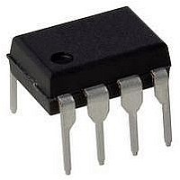
IR2125Z International Rectifier, IR2125Z Datasheet

IR2125Z
Specifications of IR2125Z
Available stocks
Related parts for IR2125Z
IR2125Z Summary of contents
Page 1
... Error lead indicates fault conditions and pro grams shutdown time n Output in phase with input Description The IR2125Z is a high voltage, high speed power MOSFET and IGBT driver with over-current limiting protection circuitry. Proprietary GVIC and latch immune CMOS technologies enable ruggedized minilithic consturction ...
Page 2
... IR2125Z Recommended Operating Conditions The Input/Output logic timing diagram is shown in Figure 1. For proper operation the device should be used within the recommended conditions. The V S offset ratings are tested with all supplies biased at 15V differential. Symbol V B High Side Floating Supply Absolute Voltage ...
Page 3
... V B -0.1 — — -0.1 — — — +0.1 — +0.1 — 9 — — — — 3 — — — IR2125Z Test Conditions 400V 0V 0V µ 20V V 10V < < 20V mV 10V < < 20V V µ 5V ERR < V ERR ERR > V ERR ...
Page 4
... IR2125Z IN CS ERR HO Figure 1. Input/Output Timing Diagram 50% 50 off t r 90% HO 10% Figure 3. Switching Time Waveform Definitions 50 90% Figure 5. CS Shutdown Waveform Definitions 4 " Figure 2. Floating Supply Voltage Transient Test Circuit t f 90% 10% Figure 4. ERR Shutdown Waveform Definitions CS ERR Figure ERR Waveform Definitions 400 V < ...
Page 5
... Figure 7B. Turn-On Time vs. Voltage 500 400 300 Max. 200 Typ. 100 0 75 100 125 10 12 Figure 8B. Turn-Off Time vs. Voltage 5.00 4.00 3.00 2.00 Max. 1.00 Typ. 0.00 75 100 125 10 Figure 9B. ERR to Output Shutdown vs. Voltage IR2125Z Supply Voltage (V) BIAS Supply Voltage (V) BIAS Supply Voltage (V) BIAS ...
Page 6
... IR2125Z 100 Max. Typ -50 - Temperature (°C) Figure 10A. Turn-On Rise Time vs. Temperature 100 Max. Typ -50 - Temperature (°C) Figure 11A. Turn-Off Fall Time vs. Temperature 15.0 12.0 Min. 9.0 6.0 3.0 0.0 -50 - Temperature (°C) Figure 12A. Logic “1” Input Threshold vs. Temperature 6 100 ...
Page 7
... Figure 14B. Logic “1” Input Threshold vs. Voltage 5.00 4.00 3.00 2.00 1.00 Max. 0.00 75 100 125 10 12 Figure 15B. Logic “0” Input Threshold vs. Voltage IR2125Z Supply Voltage (V) BIAS Logic Supply Voltage ( Logic Supply Voltage (V) ...
Page 8
... IR2125Z 500 400 Max. 300 Typ. 200 Min. 100 0 -50 - Temperature (°C) Figure 16A. CS Input Threshold (+) vs. Temperature 500 400 300 Max. Typ. 200 Min. 100 0 -50 - Temperature (°C) Figure 17A. CS Input Threshold (-) vs. Temperature 1.00 0.80 0.60 0.40 0.20 Max. 0.00 -50 -25 ...
Page 9
... Max 100 125 0 100 Figure 20B. Offset Supply Current vs. Voltage 2.00 1.60 1.20 0.80 Max. 0.40 Typ. 0. 100 125 Figure 21B. V IR2125Z Floating Supply Voltage (V) BS 200 300 400 500 V Boost Voltage ( Floating Supply Voltage (V) BS Supply Current vs. Voltage BS ...
Page 10
... IR2125Z 2.00 1.60 Max. 1.20 0.80 Typ. 0.40 0.00 -50 - Temperature (°C) Figure 22A. V Supply Current vs. Temperature Max. 5 Typ. 0 -50 - Temperature (°C) Figure 23A. Logic “1” Input Current vs. Temperature 5.00 4.00 3.00 2.00 Max. 1.00 0.00 -50 - Temperature (°C) Figure 24A. Logic “0” Input Current vs. Temperature 10 2 ...
Page 11
... Max. 1.00 0.00 75 100 125 10 12 Figure 26B. “Low” CS Bias Current vs. Voltage 11.0 10.0 Max. 9.0 Typ. 8.0 Min. 7.0 6.0 -50 -25 75 100 125 Figure 28 IR2125Z Floating Supply Voltage ( Floating Supply Voltage ( 100 125 Temperature (°C) Undervoltage (-) vs. Temperature 11 ...
Page 12
... IR2125Z 11.0 10.0 Max. Typ. 9.0 Min. 8.0 7.0 6.0 -50 - Temperature (°C) Figure 29. V Undervoltage (+) vs. Temperature CC 250 200 150 Max. Typ. 100 Min -50 - Temperature (°C) Figure 31A. ERR Timing Charge Current vs. Temperature 25.0 20.0 Typ. 15.0 Min. 10.0 5.0 0.0 -50 -25 ...
Page 13
... Typ. 1.00 Min. 0.50 0.00 75 100 125 10 12 Figure 34B. Output Source Current vs. Voltage 5.00 4.00 3.00 Typ. 2.00 Min. 1.00 0.00 75 100 125 10 12 Figure 35B. Output Sink Current vs. Voltage IR2125Z Logic Supply Voltage ( Floating Supply Voltage ( Floating Supply Voltage ( ...
Page 14
... IR2125Z 500 400 300 200 Typ. 100 0 5 7.5 10 Input Voltage (V) Figure 36A. Turn-On Time vs. Input Voltage 0.00 -3.00 -6.00 -9.00 -12.00 -15.00 Figure 37. Maximum V 14 500 V = 15V CC 400 300 200 Typ. 100 0 12 Figure 36B. Turn-Off Time vs. Input Voltage Typ. ...
Page 15
... High side floating supply return S Current sense input to current sense comparator CS www.irf.com UV DETECT R HV LEVEL R UP PULSE SHIFT FILTER SHIFTERS S PULSE V B GEN Q R PULSE DOWN FILTER SHIFTERS S HV LEVEL SHIFT IR2125Z V B PRE Q DRIVER HO BUFFER V S 0.23V - PULSE GEN + CS AMPLIFER 500ns BLANK COMPARAT OR 15 ...
Page 16
... IR2125Z Case Outline and Dimensions- MO-036AA IR WORLD HEADQUARTERS: 233 Kansas St., El Segundo, California 90245, USA Tel: (310) 252-7105 16 IR2125Z Visit us at www.irf.com for sales contact information. Data and specifications subject to change without notice. 05/01 IR2153Z TAC Fax: (310) 252-7903 www.irf.com ...


