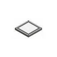
DS92LX2122SQE/NOPB National Semiconductor, DS92LX2122SQE/NOPB Datasheet - Page 31

DS92LX2122SQE/NOPB
Manufacturer Part Number
DS92LX2122SQE/NOPB
Description
IC, SERDES, 50MHz, 1.05Gbps, LLP-48
Manufacturer
National Semiconductor
Datasheet
1.DS92LX2121SQXNOPB.pdf
(38 pages)
Specifications of DS92LX2122SQE/NOPB
Serdes Function
Deserializer
Data Rate
100Kbps
No. Of Inputs
2
No. Of Outputs
21
Supply Voltage Range
3V To 3.6V
Driver Case Style
LLP
No. Of Pins
48
Msl
MSL 3 - 168 Hours
Rohs Compliant
Yes
Peak Reflow Compatible (260 C)
Yes
Leaded Process Compatible
Yes
Lead Free Status / RoHS Status
Lead free / RoHS Compliant
Lead Free Status / RoHS Status
Lead free / RoHS Compliant
Available stocks
Company
Part Number
Manufacturer
Quantity
Price
Part Number:
DS92LX2122SQE/NOPB
Manufacturer:
TI/德州仪器
Quantity:
20 000
Step 3: Stop at SPEED BIST by turning off BIST mode in the
Deserializer to determine Pass/Fail.
To end BIST, the system must pull BISTEN pin of the Dese-
rializer LOW. The BIST duration is fully defined by the BIS-
For instance, if BISTEN is held HIGH for 1 second and the
PCLK is running at 43 MHz with 16 bpp, then the Bit Error
Rate is no better than 1.46E-9.
Step 4: Place system in Normal Operating Mode by disabling
BIST at the Serializer.
Once Step 3 is complete, AT SPEED BIST is over and the
Deserializer is out of BIST mode. To fully return to Normal
mode, apply Normal input data into the Serializer.
Any PASS result will remain unless it is changed by a new
BIST session or cleared by asserting and releasing PDB. The
default state of PASS after a PDB toggle is HIGH.
It is important to note that AT SPEED BIST will only determine
if there is an issue on the link that is not related to the clock
and data recovery of the link (whose status is flagged with
LOCK pin).
FIGURE 28. BIST BER Calculation
FIGURE 27. BIST Timing Diagram
31
TEN width and thus the Bit Error Rate is determined by how
long the system holds BISTEN HIGH.
LVCMOS VDDIO OPTION
1.8V or 3.3V SER Inputs and DES Outputs are user config-
urable to provide compatibility with 1.8V and 3.3V system
interfaces.
REMOTE WAKE UP (Camera Mode)
After initial power up, the SER is in a low-power Standby
mode. The DES (controlled by the host ) 'Remote Wakeup'
register allows the DES side to generate a signal across the
link to remotely wakeup the SER. Once the SER detects the
wakeup signal, the SER switches from Standby mode to ac-
tive mode. In active mode, the SER locks onto PCLK input (if
present), otherwise the on-chip oscillator is used as the input
clock source. Note the host controller should monitor the DES
30125105
www.national.com
30125164


