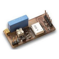
HCPL-800J Avago Technologies US Inc., HCPL-800J Datasheet - Page 15

HCPL-800J
Manufacturer Part Number
HCPL-800J
Description
IC, PLC POWERLINE DAA, SOIC-16
Manufacturer
Avago Technologies US Inc.
Datasheet
1.HCPL-800J-500.pdf
(18 pages)
Specifications of HCPL-800J
Supply Voltage Range
4.75V To 5.25V
Power Dissipation Pd
1000mW
Operating Temperature Range
-40°C To +85°C
Digital Ic Case Style
SOIC
No. Of Pins
16
No. Of Channels
1
Mounting Type
Surface Mount
Package / Case
SO-16
Current - Supply
28mA
Voltage - Supply
4.75 V ~ 5.25 V
Operating Temperature
-40°C ~ 85°C
Applications
Powerline Data Access
Lead Free Status / RoHS Status
Contains lead / RoHS non-compliant
Available stocks
Company
Part Number
Manufacturer
Quantity
Price
Company:
Part Number:
HCPL-800J
Manufacturer:
AVAGO
Quantity:
4 913
Part Number:
HCPL-800J
Manufacturer:
AVAGO/安华高
Quantity:
20 000
Company:
Part Number:
HCPL-800J#500
Manufacturer:
AVAGO
Quantity:
794
Company:
Part Number:
HCPL-800J-000E
Manufacturer:
AVAGO
Quantity:
44
Company:
Part Number:
HCPL-800J-300E
Manufacturer:
AVAGO
Quantity:
5 000
Company:
Part Number:
HCPL-800J-500E
Manufacturer:
AVAGO
Quantity:
5 000
Part Number:
HCPL-800J-500E
Manufacturer:
AVAGO/安华高
Quantity:
20 000
Applications Information
Figure 25. Schematic of HCPL - 800J application for FSK modulation scheme
Typical application for FSK modulation scheme
The HCPL-800J is designed to work with various trans-
ceivers and can be used with a variety of modulation
methods including ASK, FSK and BPSK. Figure 25 shows
a typical application in a powerline modem using
Frequency Shift Keying (FSK) modulation scheme.
Transmitter
The analogue Tx input pin is connected to the modulator
via an external coupling capacitor C1 and a series resistor
R3 (see Figure 25). Optimal performance is obtained with
an input signal of 250 µA
output signal of 0.5 V
nF, the optimal series resistor R3 would be 2 kΩ.
TX AGC
To ensure a stable and constant output voltage at Tx-PD-
out, the HCPL-800J includes an Automatic Gain Control
(AGC) circuit in the isolated transmit signal path.
This AGC circuit compensates for variations in the
input signal level presented at Tx-in and variations in
the optical channel over temperature and time. The
Tx-PD-out output signal is effectively stabilized for input
Tx-in signals of between 150 µA
Figure 8). The AGC circuit starts to function 10 µs after the
Tx-en signal is set to logic high. After a period of 180 µs
the Tx-PD-out signal typically reaches 66% of its steady
state level (see Figure 26). To ensure correct operation of
the internal circuitry, an external 1 µF capacitor needs to
be connected from pin 11 to GND2.
15
Rx-out
Status
Tx-en
Tx-in
C1
5 kÙ
10 kÙ
R1
R2
100 nF
PP
100 nF
V
100 nF
using a coupling capacitor of 100
CC1
R3
2 kÙ
PP
GND1
. E.g., for a modulator with an
GND1
PP
1
2
3
4
5
6
7
8
HCPL-800J
and 250 µA
Tx-en
Tx-in
Rx-PD-out
Rx-Amp-in
Status
Rx-out
V
GND1
CC1
Tx-PD-out
PP
Tx-LD-in
GND2
Tx-out
(see
Rx-in
V
C
R
CC2
ext
ref
16
15
14
13
12
11
10
9
The optical signal coupling technology used in the
HCPL-800J transmit path achieves very good harmonic
distortion typically HD2 < -50 dB and HD3 < -62 dB, which
is usually significantly better than the distortion perfor-
mance of the modulated input signal. However to meet
the requirements of some international EMC regulations
it is often necessary to filter the modulated input signal.
The optimal position for such a filter is between pins 13
and 12 as shown in Figure 25. A possible band-pass filter
topology is shown in Figure 27, some typical values of
the components in this filter are listed in Table 1.
Figure 26. Tx-PD-out AGC response time
GND2
Tx-PD-out 1 V/Div
Tx-en 5 V/Div
1 µF
R
24 kÙ
GND2
ref
GND2
Filter
Filter
R4
2 Ù
t
s, Tx
1 µF
100 nF
GND2
L2
D1
GND2
t
GND2
AGC
100 µF
V
CC2
L1
330 µH
C2
X2
L
N
5 0 µs/Div


