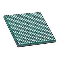
LFXP2-40E-5FN672C LATTICE SEMICONDUCTOR, LFXP2-40E-5FN672C Datasheet - Page 16

LFXP2-40E-5FN672C
Manufacturer Part Number
LFXP2-40E-5FN672C
Description
IC, LATTICEXP2 FPGA, 435MHZ, FPBGA-672
Manufacturer
LATTICE SEMICONDUCTOR
Series
LatticeXP2r
Datasheet
1.LFXP2-5E-5TN144C.pdf
(93 pages)
Specifications of LFXP2-40E-5FN672C
No. Of Logic Blocks
40000
No. Of Macrocells
20000
Family Type
LatticeXP2
No. Of Speed Grades
5
No. Of I/o's
540
Clock Management
PLL
Total Ram Bits
885Kbit
Lead Free Status / RoHS Status
Lead free / RoHS Compliant
- Current page: 16 of 93
- Download datasheet (2Mb)
Lattice Semiconductor
devices have six secondary clock regions. All devices in the LatticeXP2 family have eight secondary clock
resources per region (SC0 to SC7).
The secondary clock muxes are located in the center of the device. Figure 2-12 shows the mux structure of the
secondary clock routing. Secondary clocks SC0 to SC3 are used for high fan-out control and SC4 to SC7 are used
for clock signals.
Figure 2-11. Secondary Clock Regions XP2-40
Figure 2-12. Per Region Secondary Clock Selection
SC0
4:1
Secondary Clock
Secondary Clock
Secondary Clock
Secondary Clock
I/O Bank 0
I/O Bank 5
Region 1
SC1
Region 2
Region 3
Region 4
4:1
Secondary Clock Feedlines: 8 PIOs + 16 Routing
8 Secondary Clocks (SC0 to SC7) per Region
SC2
4:1
SC3
4:1
Clock/Control
SC4
2-13
Secondary Clock
Secondary Clock
Secondary Clock
Secondary Clock
4:1
Region 5
I/O Bank 1
Region 6
Region 7
Region 8
I/O Bank 4
SC5
4:1
SC6
4:1
LatticeXP2 Family Data Sheet
SC7
4:1
Vertical Routing
Channel Regional
Boundary
EBR Row
Regional
Boundary
EBR Row
Regional
Boundary
DSP Row
Regional
Boundary
Architecture
Related parts for LFXP2-40E-5FN672C
Image
Part Number
Description
Manufacturer
Datasheet
Request
R

Part Number:
Description:
IC, LATTICEXP2 FPGA, 435MHZ, FPBGA-484
Manufacturer:
LATTICE SEMICONDUCTOR
Datasheet:
Part Number:
Description:
ISPLSI2032-80LT44Lattice Semiconductor [In-System Programmable High Density PLD]
Manufacturer:
Lattice Semiconductor Corp.
Datasheet:
Part Number:
Description:
IC PROGRAMMED LATTICE GAL 16V8
Manufacturer:
Lattice Semiconductor Corp.
Datasheet:
Part Number:
Description:
357-036-542-201 CARDEDGE 36POS DL .156 BLK LOPRO
Manufacturer:
Lattice Semiconductor Corp.
Datasheet:
Part Number:
Description:
357-036-542-201 CARDEDGE 36POS DL .156 BLK LOPRO
Manufacturer:
Lattice Semiconductor Corp.
Datasheet:
Part Number:
Description:
357-036-542-201 CARDEDGE 36POS DL .156 BLK LOPRO
Manufacturer:
Lattice Semiconductor Corp.
Datasheet:
Part Number:
Description:
357-036-542-201 CARDEDGE 36POS DL .156 BLK LOPRO
Manufacturer:
Lattice Semiconductor Corp.
Datasheet:
Part Number:
Description:
357-036-542-201 CARDEDGE 36POS DL .156 BLK LOPRO
Manufacturer:
Lattice Semiconductor Corp.
Datasheet:
Part Number:
Description:
357-036-542-201 CARDEDGE 36POS DL .156 BLK LOPRO
Manufacturer:
Lattice Semiconductor Corp.
Datasheet:
Part Number:
Description:
357-036-542-201 CARDEDGE 36POS DL .156 BLK LOPRO
Manufacturer:
Lattice Semiconductor Corp.
Datasheet:
Part Number:
Description:
357-036-542-201 CARDEDGE 36POS DL .156 BLK LOPRO
Manufacturer:
Lattice Semiconductor Corp.
Datasheet:
Part Number:
Description:
357-036-542-201 CARDEDGE 36POS DL .156 BLK LOPRO
Manufacturer:
Lattice Semiconductor Corp.
Datasheet:
Part Number:
Description:
357-036-542-201 CARDEDGE 36POS DL .156 BLK LOPRO
Manufacturer:
Lattice Semiconductor Corp.
Datasheet:
Part Number:
Description:
In-system programmable 3.3V generic digital switch
Manufacturer:
Lattice Semiconductor Corp.
Datasheet:
Part Number:
Description:
High performance E2CMOS PLD generic array logic, 15ns, quarter power
Manufacturer:
Lattice Semiconductor Corp.
Datasheet:


