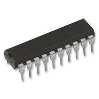
GAL16V8D15LPN LATTICE SEMICONDUCTOR, GAL16V8D15LPN Datasheet - Page 11

GAL16V8D15LPN
Manufacturer Part Number
GAL16V8D15LPN
Description
IC, GAL, 15NS, DIP-20
Manufacturer
LATTICE SEMICONDUCTOR
Datasheet
1.GAL16V8D-25QPN.pdf
(22 pages)
Specifications of GAL16V8D15LPN
Logic Type
EEPLD
Propagation Delay
15ns
No. Of I/o's
8
Frequency
62.5MHz
Supply Current Max
90mA
Supply Voltage Range
4.75V To 5.25V
Operating Temperature Range
0°C To +75°C
Logic Case Style
DIP
Lead Free Status / RoHS Status
Lead free / RoHS Compliant
1) Refer to Switching Test Conditions section.
2) Calculated from fmax with internal feedback. Refer to fmax Descriptions section.
3) Refer to fmax Descriptions section. Characterized but not 100% tested.
4) Characterized but not 100% tested.
*Characterized but not 100% tested.
PARAMETER
AC Switching Characteristics
Capacitance (T
f
SYMBOL
max
t
t
t
t
t
t
t
t
t
wh
dis
pd
co
cf
su
en
wl
h
C
C
2
3
I/O
I
COND
TEST
—
—
—
—
—
C
C
A
A
A
A
A
B
B
1
.
A
= 25 C, f = 1.0 MHz)
Input or I/O to Comb. Output
Clock to Output Delay
Clock to Feedback Delay
Setup Time, Input or Feedback before Clock
Hold Time, Input or Feedback after Clock
Maximum Clock Frequency with
External Feedback, 1/(tsu + tco)
Maximum Clock Frequency with
Internal Feedback, 1/(tsu + tcf)
Maximum Clock Frequency with
No Feedback
Clock Pulse Duration, High
Clock Pulse Duration, Low
Input or I/O to Output Enabled
OE to Output Enabled
Input or I/O to Output Disabled
OE to Output Disabled
DESCRIPTION
Input Capacitance
I/O Capacitance
PARAMETER
Over Recommended Operating Conditions
MAXIMUM*
8
8
11
Specifications GAL16V8D
UNITS
pF
pF
182
200
250
MIN. MAX.
2.5
2
—
2
—
—
—
—
1
1
0
4
4
COM
-3
3.5
2.5
4.5
4.5
4.5
4.5
—
—
— 142.8 —
—
—
—
—
3
166
166
MIN. MAX.
—
3
3
1
1
3
0
1
1
1
1
V
4
4
TEST CONDITIONS
V
COM
CC
CC
-5
= 5.0V, V
—
—
—
—
—
—
= 5.0V, V
5
4
3
6
6
5
5
COM / IND
MIN. MAX.
100
125
125
—
1
1
5
0
4
4
1
1
1
1
I/O
I
-7
= 2.0V
= 2.0V
7.5
—
—
—
—
—
—
—
5
3
9
6
9
6
UNITS
MHz
MHz
MHz
ns
ns
ns
ns
ns
ns
ns
ns
ns
ns
ns


