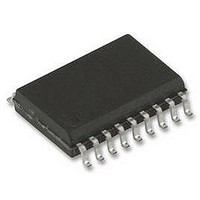
74HCT374D NXP Semiconductors, 74HCT374D Datasheet - Page 2

74HCT374D
Manufacturer Part Number
74HCT374D
Description
74HCT CMOS, SMD, 74HCT374, SOIC20
Manufacturer
NXP Semiconductors
Datasheet
1.74HCT374D.pdf
(8 pages)
Specifications of 74HCT374D
Flip-flop Type
D
Propagation Delay
16ns
Frequency
48MHz
Output Current
6mA
Supply Voltage Range
4.5V To 5.5V
Logic Case Style
SOIC
No. Of Pins
20
Operating
RoHS Compliant
Trigger Type
Positive Edge
Ic Output Type
Tri State Non Inverted
Rohs Compliant
Yes
Available stocks
Company
Part Number
Manufacturer
Quantity
Price
Part Number:
74HCT374D
Manufacturer:
NXP/恩智浦
Quantity:
20 000
Company:
Part Number:
74HCT374DB
Manufacturer:
KAWASAKI
Quantity:
10
Philips Semiconductors
FEATURES
GENERAL DESCRIPTION
The 74HC/HCT374 are high-speed Si-gate CMOS devices
and are pin compatible with low power Schottky TTL
(LSTTL). They are specified in compliance with JEDEC
standard no. 7A.
QUICK REFERENCE DATA
GND = 0 V; T
Notes
1. C
2. For HC the condition is V
ORDERING INFORMATION
See
December 1990
t
f
C
C
PHL
max
3-state non-inverting outputs for bus oriented
applications
8-bit positive, edge-triggered register
Common 3-state output enable input
Independent register and 3-state buffer operation
Output capability: bus driver
I
Octal D-type flip-flop; positive
edge-trigger; 3-state
I
PD
CC
SYMBOL
f
f
C
V
For HCT the condition is V
i
o
“74HC/HCT/HCU/HCMOS Logic Package Information”
/ t
CC
PD
L
category: MSI
= output frequency in MHz
= input frequency in MHz
(C
PLH
= output load capacitance in pF
P
is used to determine the dynamic power dissipation (P
= supply voltage in V
L
D
= C
V
amb
CC
PD
2
= 25 C; t
propagation delay CP to Q
maximum clock frequency
input capacitance
power dissipation capacitance per flip-flop
V
f
o
CC
) = sum of outputs
2
f
r
i
= t
I
I
f
= GND to V
= GND to V
= 6 ns
(C
PARAMETER
L
V
CC
2
CC
CC
n
f
o
) where:
1.5 V
2
.
The 74HC/HCT374 are octal D-type flip-flops featuring
separate D-type inputs for each flip-flop and 3-state
outputs for bus oriented applications. A clock (CP) and an
output enable (OE) input are common to all flip-flops.
The 8 flip-flops will store the state of their individual
D-inputs that meet the set-up and hold times requirements
on the LOW-to-HIGH CP transition.
When OE is LOW, the contents of the 8 flip-flops are
available at the outputs. When OE is HIGH, the outputs go
to the high impedance OFF-state. Operation of the
OE input does not affect the state of the flip-flops.
The “374” is functionally identical to the “534”, but has
non-inverting outputs.
D
C
notes 1 and 2
in W):
L
= 15 pF; V
CONDITIONS
CC
= 5 V
74HC/HCT374
15
77
3.5
17
Product specification
HC
TYPICAL
13
48
3.5
17
HCT
ns
MHz
pF
pF
UNIT


