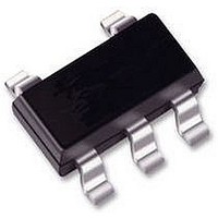
74LVC1GU04GW NXP Semiconductors, 74LVC1GU04GW Datasheet - Page 3

74LVC1GU04GW
Manufacturer Part Number
74LVC1GU04GW
Description
IC, LOGIC, 74LVC1G, INVERTER, UMT5
Manufacturer
NXP Semiconductors
Datasheet
1.74LVC1GU04GW.pdf
(18 pages)
Specifications of 74LVC1GU04GW
Output Current
32mA
No. Of Inputs
1
Supply Voltage Range
1.65V To 5.5V
Logic Case Style
SOT-353
No. Of Pins
5
Operating Temperature Range
-40°C To +125°C
Svhc
No
Logic Type
Inverter Gate
Lead Free Status / RoHS Status
Lead free / RoHS Compliant
Available stocks
Company
Part Number
Manufacturer
Quantity
Price
Company:
Part Number:
74LVC1GU04GW
Manufacturer:
NXP
Quantity:
3 000
Part Number:
74LVC1GU04GW
Manufacturer:
NXP/恩智浦
Quantity:
20 000
Company:
Part Number:
74LVC1GU04GW,125
Manufacturer:
NXP Semiconductors
Quantity:
4 750
Company:
Part Number:
74LVC1GU04GWЈ¬125
Manufacturer:
NXP
Quantity:
12 000
NXP Semiconductors
Table 3.
7. Functional description
Table 4.
[1]
8. Limiting values
Table 5.
In accordance with the Absolute Maximum Rating System (IEC 60134). Voltages are referenced to GND (ground = 0 V).
[1]
[2]
[3]
74LVC1GU04
Product data sheet
Symbol
n.c.
A
GND
Y
n.c.
V
Input (A)
L
H
Symbol
V
I
V
I
V
I
I
I
P
T
IK
OK
O
CC
GND
stg
CC
CC
I
O
tot
H = HIGH voltage level; L = LOW voltage level.
The input and output voltage ratings may be exceeded if the input and output current ratings are observed.
When V
For TSSOP5 and SC-74A packages: above 87.5 °C the value of P
For XSON6 packages: above 118 °C the value of P
CC
Pin description
Function table
Limiting values
Parameter
supply voltage
input clamping current
input voltage
output clamping current
output voltage
output current
supply current
ground current
total power dissipation
storage temperature
Pin
SOT353-1, SOT753 SOT886, SOT891, SOT1115 and SOT1202
1
2
3
4
-
5
= 0 V (Power-down mode), the output voltage can be 5.5 V in normal operation.
6.2 Pin description
[1]
1
2
3
4
5
6
All information provided in this document is subject to legal disclaimers.
V
V
Active mode
V
Conditions
T
amb
I
O
O
< 0 V
tot
Rev. 9 — 21 October 2010
> V
= 0 V to V
= −40 °C to +125 °C
derates linearly with 7.8 mW/K.
CC
or V
CC
O
Output (Y)
H
L
< 0 V
tot
derates linearly with 4.0 mW/K.
[1][2]
[1]
[3]
Description
not connected
data input A
ground (0 V)
data output Y
not connected
supply voltage
Min
−0.5
-
−0.5
-
−0.5
-
-
-
-
−65
74LVC1GU04
Max
+6.5
−50
+6.5
±50
V
±50
+100
−100
250
+150
CC
© NXP B.V. 2010. All rights reserved.
+ 0.5
Inverter
Unit
V
mA
V
mA
V
mA
mA
mA
mW
°C
3 of 18


