SST39VF020-70-4C-NHE SILICON STORAGE TECHNOLOGY, SST39VF020-70-4C-NHE Datasheet - Page 7
SST39VF020-70-4C-NHE
Manufacturer Part Number
SST39VF020-70-4C-NHE
Description
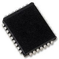
2M FLASH MEMORY, 4KB SECTOR, PLCC32
Manufacturer
SILICON STORAGE TECHNOLOGY
Datasheet
1.SST39VF040-70-4C-NHE.pdf
(25 pages)
Specifications of SST39VF020-70-4C-NHE
Memory Size
2Mbit
Supply Voltage Range
2.7V To 3.6V
Memory Case Style
PLCC
No. Of Pins
32
Svhc
No SVHC (18-Jun-2010)
Access Time
70ns
Interface
X8 MPF
Memory Configuration
256K X 8bit
Memory Type
Flash - NOR
Operating Temperature Range
0°C To +70°C
Rohs Compliant
Yes
Lead Free Status / RoHS Status
Lead free / RoHS Compliant
Available stocks
Company
Part Number
Manufacturer
Quantity
Price
Company:

Part Number:
SST39VF020-70-4C-NHE
Manufacturer:
SST
Quantity:
6 249
Company:
Part Number:
SST39VF020-70-4C-NHE
Manufacturer:
Microchip Technology
Quantity:
10 000
Company:
Part Number:
SST39VF020-70-4C-NHE-T
Manufacturer:
Microchip Technology
Quantity:
10 000


512 Kbit / 1 Mbit / 2 Mbit / 4 Mbit Multi-Purpose Flash
SST39LF512 / SST39LF010 / SST39LF020 / SST39LF040
SST39VF512 / SST39VF010 / SST39VF020 / SST39VF040
TABLE 4: S
Absolute Maximum Stress Ratings (Applied conditions greater than those listed under “Absolute Maximum Stress
Ratings” may cause permanent damage to the device. This is a stress rating only and functional operation of the device at
these conditions or conditions greater than those defined in the operational sections of this data sheet is not implied. Expo-
sure to absolute maximum stress rating conditions may affect device reliability.)
Temperature Under Bias . . . . . . . . . . . . . . . . . . . . . . . . . . . . . . . . . . . . . . . . . . . . . . . . . . . . . . . . . . . . . . . . . . . . -55°C to +125°C
Storage Temperature . . . . . . . . . . . . . . . . . . . . . . . . . . . . . . . . . . . . . . . . . . . . . . . . . . . . . . . . . . . . . . . . . . . . . . . -65°C to +150°C
D. C. Voltage on Any Pin to Ground Potential . . . . . . . . . . . . . . . . . . . . . . . . . . . . . . . . . . . . . . . . . . . . . . . . . . -0.5V to V
Transient Voltage (<20 ns) on Any Pin to Ground Potential . . . . . . . . . . . . . . . . . . . . . . . . . . . . . . . . . . . . . . -2.0V to V
Voltage on A
Package Power Dissipation Capability (Ta = 25°C) . . . . . . . . . . . . . . . . . . . . . . . . . . . . . . . . . . . . . . . . . . . . . . . . . . . . . . . . 1.0W
Surface Mount Solder Reflow Temperature
Output Short Circuit Current
O
O
©2005 Silicon Storage Technology, Inc.
Command
Sequence
Byte-Program
Sector-Erase
Chip-Erase
Software ID Entry
Software ID Exit
Software ID Exit
Range
Commercial
Range
Commercial
Industrial
PERATING
PERATING
1. Address format A
2. BA = Program Byte address
3. SA
4. The device does not remain in Software Product ID mode if powered down.
5. With A
6. Both Software ID Exit operations are equivalent
1. Excluding certain with-Pb 32-PLCC units, all packages are 260
2. Outputs shorted for no more than one second. No more than one output shorted at a time.
Certain with-Pb 32-PLCC package types are capable of 240
X
for Sector-Erase; uses A
MS
Address A
Addresses A
A
A
9
R
R
MS
MS
-A
Pin to Ground Potential . . . . . . . . . . . . . . . . . . . . . . . . . . . . . . . . . . . . . . . . . . . . . . . . . . . . . . . . . . .-0.5V to 13.2V
ANGE FOR
ANGE FOR
OFTWARE
1
= Most significant address
= A
6
6
= 0; SST Manufacturer’s ID = BFH, is read with A
4,5
15
14
15
for SST39LF/VF512, A
SST39LF/VF512 Device ID = D4H, is read with A
SST39LF/VF010 Device ID = D5H, is read with A
SST39LF/VF020 Device ID = D6H, is read with A
SST39LF/VF040 Device ID = D7H, is read with A
-A
MS
can be V
Ambient Temp
Ambient Temp
-40°C to +85°C
5555H
5555H
5555H
5555H
5555H
Addr
0
0°C to +70°C
0°C to +70°C
Write Cycle
XXH
-A
C
(Hex),
SST39LF512/010/020/040
SST39VF512/010/020/040
1st Bus
15
OMMAND
2
1
can be V
. . . . . . . . . . . . . . . . . . . . . . . . . . . . . . . . . . . . . . . . . . . . . . . . . . . . . . . . . . . . . . . . . . . . . . . . . 50 mA
IL
MS
or V
Data
AAH
AAH
AAH
AAH
AAH
F0H
-A
12
IH
IL
address lines
S
, but no other value, for the Command sequence for SST39LF/VF512.
or V
EQUENCE
2AAAH
2AAAH
2AAAH
2AAAH
2AAAH
16
Addr
Write Cycle
IH
1
for SST39LF/VF010, A
2nd Bus
, but no other value, for the Command sequence.
. . . . . . . . . . . . . . . . . . . . . . . . . . . . . . . . . . . . . . . . . . . . . . . . .260°C for 10 seconds
1
3.0-3.6V
2.7-3.6V
2.7-3.6V
V
V
DD
DD
Data
55H
55H
55H
55H
55H
5555H
°
5555H
5555H
5555H
5555H
Addr
Write Cycle
C for 10 seconds; please consult the factory for the latest information.
°
3rd Bus
0
7
C capable in both non-Pb and with-Pb solder versions.
= 0,
17
1
AC C
0
0
0
0
for SST39LF/VF020, and A
Input Rise/Fall Time . . . . . . . . . . . . . . . 5 ns
Output Load
See Figures 14 and 15
= 1,
= 1,
= 1,
= 1.
Data
A0H
F0H
80H
80H
90H
C
C
ONDITIONS OF
L
L
= 30 pF for SST39LF512/010/020/040
= 100 pF for SST39VF512/010/020/040
5555H
5555H
Addr
Write Cycle
BA
4th Bus
2
1
Data
Data
AAH
AAH
T
EST
18
for SST39LF/VF040
2AAAH
2AAAH
Addr
Write Cycle
5th Bus
1
Data
55H
55H
S71150-09-000
5555H
Addr
SA
Write Cycle
Data Sheet
6th Bus
X
3
1
DD
DD
T4.2 1150
Data
+0.5V
+2.0V
30H
10H
1/06
Related parts for SST39VF020-70-4C-NHE
Image
Part Number
Description
Manufacturer
Datasheet
Request
R

Part Number:
Description:
512 Kbit/1 Mbit (x8) multi-purpose flash
Manufacturer:
Silicon Storage Technology, Inc
Datasheet:
Part Number:
Description:
512 Kbit/1 Mbit (x8) multi-purpose flash
Manufacturer:
Silicon Storage Technology, Inc
Datasheet:
Part Number:
Description:
512 Kbit/1 Mbit (x8) multi-purpose flash
Manufacturer:
Silicon Storage Technology, Inc
Datasheet:
Part Number:
Description:
Manufacturer:
Silicon Storage Technology, Inc
Datasheet:
Part Number:
Description:
Manufacturer:
Silicon Storage Technology, Inc
Datasheet:

Part Number:
Description:
2M FLASH MEMORY, 4KB SECTOR, TSOP32
Manufacturer:
SILICON STORAGE TECHNOLOGY
Datasheet:

Part Number:
Description:
MEMORY, FLASH, 2MBIT, PARL, 32PLCC
Manufacturer:
SILICON STORAGE TECHNOLOGY
Datasheet:
Part Number:
Description:
MEMORY, FLASH, 2MBIT, PARL, 32TSOP
Manufacturer:
SILICON STORAGE TECHNOLOGY
Datasheet:
Part Number:
Description:
4 Mbit firmware hub
Manufacturer:
Silicon Storage Technology, Inc
Datasheet:
Part Number:
Description:
Manufacturer:
Silicon Storage Technology, Inc
Datasheet:
Part Number:
Description:
1 Mbit (128K x 8) page-mode EEPROM
Manufacturer:
Silicon Storage Technology, Inc
Datasheet:
Part Number:
Description:
1 Mbit (128K x 8) page-mode EEPROM
Manufacturer:
Silicon Storage Technology, Inc
Datasheet: