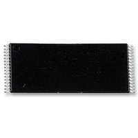
SST49LF016C-33-4C-WHE SILICON STORAGE TECHNOLOGY, SST49LF016C-33-4C-WHE Datasheet - Page 11

SST49LF016C-33-4C-WHE
Manufacturer Part Number
SST49LF016C-33-4C-WHE
Description
MEMORY, FLASH, 16M, SERIAL, 32TSOP
Manufacturer
SILICON STORAGE TECHNOLOGY
Datasheet
1.SST49LF016C-33-4C-EIE.pdf
(36 pages)
Specifications of SST49LF016C-33-4C-WHE
Memory Size
16Mbit
Clock Frequency
33MHz
Supply Voltage Range
3V To 3.6V
Memory Case Style
TSOP
No. Of Pins
32
Operating Temperature Range
0°C To +70°C
Svhc
No SVHC (18-Jun-2010)
Memory Type
Flash
Memory Configuration
2M X 8
Interface Type
Serial
Rohs Compliant
Yes
Lead Free Status / RoHS Status
Lead free / RoHS Compliant
Available stocks
Company
Part Number
Manufacturer
Quantity
Price
Company:
Part Number:
SST49LF016C-33-4C-WHE
Manufacturer:
Microchip Technology
Quantity:
135
16 Mbit LPC Serial Flash
SST49LF016C
Firmware Memory Write Cycle
TABLE 5: Firmware Memory Write Cycle
©2008 Silicon Storage Technology, Inc.
FIGURE 7: Firmware Memory Write Cycle Waveform
1. Field contents are valid on the rising edge of the present clock cycle.
Clock
Cycle
(A+1)
(A+2)
(A+3)
(A+4)
(A+5)
11-A
LFRAME#
3-9
10
1
2
LAD[3:0]
LCLK
MADDR
RSYNC
START
MSIZE
IDSEL
Name
Field
DATA
TAR0
TAR1
TAR0
TAR1
1110b 0000b
Start
IDSEL
A[27:24]
Field Contents
0000 to 1111
1111 (float)
1111 (float)
A[23:20] A[19:16]
LAD[3:0]
YYYY
KKKK
ZZZZ
1110
1111
0000
1111
1
MADDR
A[15:12]
A[11:8]
OUT then Float
Float then OUT The SST49LF016C takes control of the bus during this
IN then Float
Float then IN
Direction
LAD[3:0]
A[7:4]
OUT
IN
IN
IN
IN
IN
11
A[3:0]
MSIZE
KKKKb
Comments
LFRAME# must be active (low) for the part to respond.
Only the last start field (before LFRAME# transitions
high) will be recognized. The START field contents
(1110b) indicate a Firmware Memory Write cycle.
Indicates which SST49LF016C device should respond.
If the IDSEL (ID select) field matches the value of
ID[3:0], then that particular device will respond to the
whole bus cycle.
These seven clock cycles make up the 28-bit memory
address. YYYY is one nibble of the entire address.
Addresses are transferred most-significant nibble first.
transferred during multi-byte operations.
Device supports 1, 2, and 4 Bytes write with MSIZE =
0, 1, or 2, and KKKK=0000b, 0001b, or 0010b.
A=(10+2
Least significant nibble entered first.
‘1’s and then floats the bus prior to the next clock cycle.
This is the first part of the bus “turnaround cycle.”
A=(10+2
cycle.
A=(10+2
“ready sync” (RSYNC) and outputs the values 0000,
indicating that it has received data or a flash command.
A=(10+2
all ‘1’s and then floats the bus prior to the next clock
cycle. This is the first part of the bus “turnaround
cycle”. A=(10+2
The host resumes control of the bus during this cycle.
A=(10+2
The MSIZE field indicates how many bytes will be
In this clock cycle, the master has driven the bus to all
During this clock cycle, the SST49LF016C generates a
In this clock cycle, the SST49LF016C drives the bus to
D
0
[3:0]
D
0
[7:4]
n+1
n+1
n+1
n+1
n+1
DATA
); n = MSIZE
); n = MSIZE
); n = MSIZE
); n = MSIZE
); n = MSIZE
n+1
Dn[3:0]
); n = MSIZE
Dn[7:4]
TAR0
1111b
Tri-State
TAR1
RSYNC
S71237-08-000
0000b
1237 F04.0
TAR
Data Sheet
T5.0 1237
5/08


