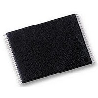
AM29F400BT-55EF Spansion Inc., AM29F400BT-55EF Datasheet - Page 14

AM29F400BT-55EF
Manufacturer Part Number
AM29F400BT-55EF
Description
IC, FLASH, 4MBIT, 55NS, TSOP-48
Manufacturer
Spansion Inc.
Datasheet
1.AM29F400BB-70EF.pdf
(43 pages)
Specifications of AM29F400BT-55EF
Memory Type
Flash
Memory Size
4Mbit
Memory Configuration
512K X 8 / 256K X 16
Access Time
55ns
Supply Voltage Range
4.75V To 5.25V
Memory Case Style
TSOP
No. Of Pins
48
Cell Type
NOR
Density
4Mb
Access Time (max)
55ns
Interface Type
Parallel
Boot Type
Top
Address Bus
19/18Bit
Operating Supply Voltage (typ)
5V
Operating Temp Range
-40C to 85C
Package Type
TSOP
Program/erase Volt (typ)
4.75 to 5.25V
Sync/async
Asynchronous
Operating Temperature Classification
Industrial
Operating Supply Voltage (min)
4.5V
Operating Supply Voltage (max)
5.5V
Word Size
8/16Bit
Number Of Words
512K/256K
Supply Current
50mA
Mounting
Surface Mount
Pin Count
48
Lead Free Status / Rohs Status
Compliant
Hardware Data Protection
The command sequence requirement of unlock cycles
for programming or erasing provides data protection
against inadver tent writes (refer to Table 5 for
command definitions). In addition, the following hard-
ware data protection measures prevent accidental
erasure or programming, which might otherwise be
caused by spurious system level signals during V
power-up and power-down transitions, or from system
noise.
Low V
When V
accept any write cycles. This protects data during V
power-up and power-down. The command register and
all internal program/erase circuits are disabled, and the
device resets. Subsequent writes are ignored until V
is greater than V
12
CC
CC
Write Inhibit
is less than V
LKO
. The system must provide the
LKO
, the device does not
D A T A
Am29F400B
CC
CC
CC
S H E E T
proper signals to the control pins to prevent uninten-
tional writes when V
Write Pulse “Glitch” Protection
Noise pulses of less than 5 ns (typical) on OE#, CE# or
WE# do not initiate a write cycle.
Logical Inhibit
Write cycles are inhibited by holding any one of OE# =
V
CE# and WE# must be a logical zero while OE# is a
logical one.
Power-Up Write Inhibit
If WE# = CE# = V
device does not accept commands on the rising edge
of WE#. The internal state machine is automatically
reset to reading array data on power-up.
IL
, CE# = V
IH
or WE# = V
IL
and OE# = V
CC
is greater than V
IH
21505E8 November 11, 2009
. To initiate a write cycle,
IH
during power up, the
LKO
.


