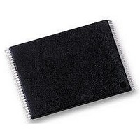
M29DW323DB70N6E STMicroelectronics, M29DW323DB70N6E Datasheet - Page 48

M29DW323DB70N6E
Manufacturer Part Number
M29DW323DB70N6E
Description
IC, FLASH, 32MBIT, 70NS, TSOP-48
Manufacturer
STMicroelectronics
Datasheet
1.M29DW323DB70N6E.pdf
(49 pages)
Specifications of M29DW323DB70N6E
Memory Type
Flash - Boot Block
Memory Size
32Mbit
Memory Configuration
4M X 8 / 2M X 16
Ic Interface Type
Parallel
Access Time
70ns
Supply Voltage Range
2.7V To 3.6V
Memory Case Style
TSOP
Lead Free Status / RoHS Status
Lead free / RoHS Compliant
Available stocks
Company
Part Number
Manufacturer
Quantity
Price
Company:
Part Number:
M29DW323DB70N6E
Manufacturer:
VISHAY
Quantity:
6 700
Part Number:
M29DW323DB70N6E
Manufacturer:
ST
Quantity:
20 000
M29DW323DT, M29DW323DB
REVISION HISTORY
Table 31. Document Revision History
48/49
20-Sep-2001
07-May-2003
26-Oct-2001
16-Jan-2002
19-Apr-2002
24-Apr-2002
08-Apr-2003
25-Jun-2003
19-Jul-2002
Date
Version
-06
-01
-02
-03
-04
-05
6.1
6.2
7.0
First Issue (Target Specification)
Document expanded to full Product Preview
Corrections made in “Primary Algorithm-Specific Extended Query” Table in Appendix-B
Description of Ready/Busy signal clarified (and Figure 15 modified)
Clarified allowable commands during block erase
Clarified the mode the device returns to in the CFI Read Query command section
tPLYH (time to reset device) re-specified.
Values for addresses 23h and 25h corrected in CFI Query System Interface Information
table in Appendix B
When in Extended Block mode, the block at the boot block address can be used as OTP.
Data Toggle Flow chart corrected. Document promoted from “Product Preview” to
“Preliminary Data”.
Revision numbering modified: a minor revision will be indicated by incrementing the digit
after the dot, and a major revision, by incrementing the digit before the dot (revision
version 06 equals 6.0).
Revision History moved to end of document.
TFBGA48, 6 x 8mm, 0.80mm pitch package added. Identification Current I
from Table 12, DC Characteristics. Erase Suspend Latency time and Data Retention
parameters and notes added to Table 7, Program, Erase Times and Program, Erase
Endurance Cycles.
Appendix C, EXTENDED MEMORY BLOCK, added. Auto Select Command sued to read
the Extended Memory Block. Extended Memory Block Verify Code row added to Tables 3
and 4, Bus Operations, BYTE = V
modified in Auto Select Command. Chip Erase Address modified in Table 8, Status
Register Bits. V
Information Scheme.
Table 17, TSOP48 Lead Plastic Thin Small Outline, 12x20 mm, Package Mechanical
Data and Figure 17, TSOP48 Lead Plastic Thin Small Outline, 12x20 mm, Bottom View
Package Outline, corrected.
Document promoted from Preliminary Data to full Datasheet status. Packing option added
to Table 20, Ordering Information Scheme.
SS
pin connection to ground clarified. Note added to Table 20, Ordering
IL
Revision Details
and Bus Operations, BYTE = V
IH
. Bank Address
ID
removed


