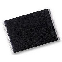
M29DW323DT70N6E STMicroelectronics, M29DW323DT70N6E Datasheet - Page 40

M29DW323DT70N6E
Manufacturer Part Number
M29DW323DT70N6E
Description
IC, FLASH, 32MBIT, 70NS, TSOP-48
Manufacturer
STMicroelectronics
Datasheet
1.M29DW323DB70N6E.pdf
(49 pages)
Specifications of M29DW323DT70N6E
Memory Type
Flash - Boot Block
Memory Size
32Mbit
Memory Configuration
4M X 8 / 2M X 16
Ic Interface Type
Parallel
Access Time
70ns
Supply Voltage Range
2.7V To 3.6V
Memory Case Style
TSOP
Lead Free Status / RoHS Status
Lead free / RoHS Compliant
Available stocks
Company
Part Number
Manufacturer
Quantity
Price
Company:
Part Number:
M29DW323DT70N6E
Manufacturer:
OMRON
Quantity:
1 200
Part Number:
M29DW323DT70N6E
Manufacturer:
ST
Quantity:
20 000
M29DW323DT, M29DW323DB
Table 25. CFI Query System Interface Information
Table 26. Device Geometry Definition
Note: The region information contained in addresses 2Dh to 34h (or 5Ah to 68h) is correct for the M29DW323DB. For the M29DW323DT the
40/49
1Ch
1Dh
1Bh
1Eh
1Fh
x16
20h
21h
22h
23h
24h
25h
26h
2Ah
2Bh
2Ch
2Dh
2Eh
x16
27h
28h
29h
2Fh
30h
31h
32h
33h
34h
regions must be reversed.
Address
Address
3Ah
3Ch
3Eh
4Ah
4Ch
36h
38h
40h
42h
44h
46h
48h
x8
4Eh
5Ah
5Ch
5Eh
50h
52h
54h
56h
58h
60h
62h
64h
66h
68h
x8
00B5h
00C5h
000Ah
0027h
0036h
0004h
0000h
0000h
0004h
0000h
0003h
0000h
Data
0016h
0002h
0000h
0000h
0000h
0002h
0007h
0000h
0020h
0000h
003Eh
0000h
0000h
0001h
Data
V
V
V
V
Typical timeout per single byte/word program = 2
Typical timeout for minimum size write buffer program = 2
Typical timeout per individual block erase = 2
Typical timeout for full chip erase = 2
Maximum timeout for byte/word program = 2
Maximum timeout for write buffer program = 2
Maximum timeout per individual block erase = 2
Maximum timeout for chip erase = 2
CC
CC
PP
PP
bit 7 to 4
bit 3 to 0
bit 7 to 4
bit 3 to 0
bit 7 to 4
bit 3 to 0
bit 7 to 4
bit 3 to 0
[Programming] Supply Minimum Program/Erase voltage
[Programming] Supply Maximum Program/Erase voltage
Device Size = 2
Flash Device Interface Code description
Maximum number of bytes in multi-byte program or page = 2
Number of Erase Block Regions. It specifies the number of
regions containing contiguous Erase Blocks of the same size.
Region 1 Information
Number of identical size erase block = 0007h+1
Region 1 Information
Block size in Region 1 = 0020h * 256 byte
Region 2 Information
Number of identical size erase block = 003Eh+1
Region 2 Information
Block size in Region 2 = 0100h * 256 byte
Logic Supply Minimum Program/Erase voltage
Logic Supply Maximum Program/Erase voltage
BCD value in volts
BCD value in 100 mV
BCD value in volts
BCD value in 100 mV
HEX value in volts
BCD value in 100 mV
HEX value in volts
BCD value in 100 mV
n
in number of bytes
Description
Description
n
n
times typical
ms
n
n
n
times typical
ms
times typical
n
n
times typical
µs
n
µs
n
256 µs
Value
11.5V
12.5V
16µs
2.7V
3.6V
4 MByte
64Kbyte
NA
NA
NA
NA
8 s
x8, x16
8Kbyte
1s
Async.
Value
NA
63
2
8


