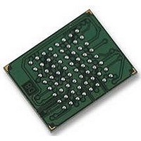
S29GL032N90FFI030 Spansion Inc., S29GL032N90FFI030 Datasheet - Page 37

S29GL032N90FFI030
Manufacturer Part Number
S29GL032N90FFI030
Description
IC, FLASH, 32MBIT, 90NS, BGA-64
Manufacturer
Spansion Inc.
Datasheet
1.S29GL032N90TFI010.pdf
(81 pages)
Specifications of S29GL032N90FFI030
Memory Type
Flash
Memory Size
32Mbit
Ic Interface Type
CFI, Parallel
Access Time
90ns
Supply Voltage Range
2.7V To 3.6V
Memory Case Style
BGA
No. Of Pins
64
Lead Free Status / RoHS Status
Lead free / RoHS Compliant
9. Common Flash Memory Interface (CFI)
October 29, 2008 S29GL-N_01_12
8.17.2
8.17.3
8.17.4
Write Pulse Glitch Protection
Logical Inhibit
Power-Up Write Inhibit
Noise pulses of less than 3 ns (typical) on OE#, CE# or WE# do not initiate a write cycle.
Write cycles are inhibited by holding any one of OE# = V
CE# and WE# must be a logical zero while OE# is a logical one.
If WE# = CE# = V
edge of WE#. The internal state machine is automatically reset to the read mode on power-up.
The Common Flash Interface (CFI) specification outlines device and host system software interrogation
handshake, which allows specific vendor-specified software algorithms to be used for entire families of
devices. Software support can then be device-independent, JEDEC ID-independent, and forward- and
backward-compatible for the specified flash device families. Flash vendors can standardize their existing
interfaces for long-term compatibility.
This device enters the CFI Query mode when the system writes the CFI Query command, 98h, to address
55h, any time the device is ready to read array data. The system can read CFI information at the addresses
given in
the reset command.
The system can also write the CFI query command when the device is in the autoselect mode. The device
enters the CFI query mode, and the system can read CFI data at the addresses given in
Table 9.1 on page 37
to reading array data.
For further information, please refer to the CFI Specification and CFI Publication 100. Alternatively, contact
your sales representative for copies of these documents.
Addresses (x16)
10h
11h
12h
13h
14h
15h
16h
17h
18h
19h
1Ah
Table 9.1 on page 37
IL
and OE# = V
Addresses (x8)
–
Table 9.4 on page
D a t a
2Ch
20h
22h
24h
26h
28h
2Ah
2Eh
30h
32h
34h
S29GL-N MirrorBit
–
Table 9.4 on page
IH
Table 9.1 CFI Query Identification String
S h e e t
during power up, the device does not accept commands on the rising
40. The system must write the reset command to return the device
0051h
0052h
0059h
0002h
0000h
0040h
0000h
0000h
0000h
0000h
0000h
Data
®
Flash Family
40. To terminate reading CFI data, the system must write
Description
Query Unique ASCII string “QRY”
Primary OEM Command Set
Address for Primary Extended Table
Alternate OEM Command Set (00h = none exists)
Address for Alternate OEM Extended Table (00h = none
exists)
IL
, CE# = V
IH
or WE# = V
IH
. To initiate a write cycle,
37


