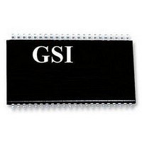
GS74108AGP-10I GSI TECHNOLOGY, GS74108AGP-10I Datasheet - Page 5

GS74108AGP-10I
Manufacturer Part Number
GS74108AGP-10I
Description
4MB ASYNCH SRAM 512K X 8, 10NS, SMD
Manufacturer
GSI TECHNOLOGY
Datasheet
1.GS74108AGP-10I.pdf
(13 pages)
Specifications of GS74108AGP-10I
Memory Size
4Mbit
Access Time
10ns
Supply Voltage Range
3V To 3.6V
Memory Case Style
TSOP-2
No. Of Pins
44
Operating Temperature Range
-40°C To +85°C
Operating Temperature Max
85°C
Memory Configuration
512K X 8
Rohs Compliant
Yes
Lead Free Status / RoHS Status
Lead free / RoHS Compliant
AC Test Conditions
AC Characteristics
Read Cycle
* These parameters are sampled and are not 100% tested.
Rev: 1.07 1/2006
Specifications cited are subject to change without notice. For latest documentation see http://www.gsitechnology.com.
Notes:
1.
2.
3.
Include scope and jig capacitance.
Test conditions as specified with output loading as shown in Fig. 1
unless otherwise noted.
Output load 2 for t
Output disable to output in High Z (OE)
Output reference level
Output enable to output in low Z (OE)
Chip disable to output in High Z (CE)
Input reference level
Chip enable to output in low Z (CE)
Output enable to output valid (OE)
Output hold from address change
Input high level
Input low level
Input rise time
Chip enable access time (CE)
Parameter
Input fall time
Output load
Address access time
Read cycle time
Parameter
LZ
, t
HZ
, t
OLZ
and t
OHZ
Conditions
V
V
tr = 1 V/ns
tf = 1 V/ns
Fig. 1& 2
IH
IL
1.4 V
1.4 V
= 0.4 V
= 2.4 V
Symbol
5/13
t
t
t
OHZ
t
t
t
t
OLZ
t
t
HZ
LZ
RC
AC
OE
OH
AA
*
*
*
*
Min
—
—
—
—
—
8
3
3
0
-8
Max
3.5
3.5
—
—
—
—
8
8
4
DQ
Min
10
—
—
—
—
—
3
3
0
-10
DQ
Max
10
10
—
—
—
—
Output Load 1
Output Load 2
4
5
4
© 2001, Giga Semiconductor, Inc.
5pF
Min
VT = 1.4 V
12
—
—
—
—
—
3
3
0
1
GS74108ATP/J/X
3.3 V
-12
50Ω
589Ω
434Ω
Max
12
12
—
—
—
—
5
6
5
30pF
1
Unit
ns
ns
ns
ns
ns
ns
ns
ns
ns


