PIC24FJ256GB106-I/MR Microchip Technology, PIC24FJ256GB106-I/MR Datasheet - Page 9
PIC24FJ256GB106-I/MR
Manufacturer Part Number
PIC24FJ256GB106-I/MR
Description
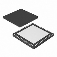
IC, 16BIT MCU, PIC24F, 32MHZ, QFN-64
Manufacturer
Microchip Technology
Series
PIC® 24Fr
Datasheets
1.PIC24FJ128GA106-IPT.pdf
(52 pages)
2.PIC24FJ64GB106-IPT.pdf
(16 pages)
3.PIC24FJ64GB106-IPT.pdf
(352 pages)
4.PIC24FJ192GB108-IPT.pdf
(328 pages)
Specifications of PIC24FJ256GB106-I/MR
Controller Family/series
PIC24
No. Of I/o's
51
Ram Memory Size
16KB
Cpu Speed
32MHz
No. Of Timers
5
Core Size
16 Bit
Program Memory Size
256KB
Peripherals
ADC, Comparator, PWM, RTC, Timer
Core Processor
PIC
Speed
32MHz
Connectivity
I²C, SPI, UART/USART, USB OTG
Number Of I /o
51
Program Memory Type
FLASH
Ram Size
16K x 8
Voltage - Supply (vcc/vdd)
2 V ~ 3.6 V
Data Converters
A/D 16x10b
Oscillator Type
Internal
Operating Temperature
-40°C ~ 85°C
Package / Case
64-VFQFN, Exposed Pad
Processor Series
PIC24FJ
Core
PIC
Data Bus Width
16 bit
Data Ram Size
16 KB
Interface Type
I2C, SPI, UART
Maximum Clock Frequency
32 MHz
Number Of Programmable I/os
52
Number Of Timers
5
Maximum Operating Temperature
+ 85 C
Mounting Style
SMD/SMT
3rd Party Development Tools
52713-733, 52714-737, 53276-922, EWDSPIC
Development Tools By Supplier
PG164130, DV164035, DV244005, DV164005, PG164120, DM240001, DM240011
Minimum Operating Temperature
- 40 C
On-chip Adc
10 bit, 16 Channel
Lead Free Status / RoHS Status
Lead free / RoHS Compliant
For Use With
876-1004 - PIC24 BREAKOUT BOARD
Eeprom Size
-
Lead Free Status / Rohs Status
Details
Available stocks
Company
Part Number
Manufacturer
Quantity
Price
Company:

Part Number:
PIC24FJ256GB106-I/MR
Manufacturer:
TI
Quantity:
1 292


28. Module: Oscillator (LPRC)
29. Module: Oscillator (Two-Speed Start-up)
2010 Microchip Technology Inc.
The LPRC may not automatically restart follow-
ing BOR events (i.e., when supply voltage sags
to between the BOR and POR thresholds, then
returns to above the BOR level). When this
happens, systems that use the LPRC clock may
not work. This includes the PLL, Two-Speed
Start-up, Fail-Safe Clock Monitor and the WDT.
Work around
For PLL issues: select a non-PLL Clock mode
as the initial start-up mode, using the FNOSC
Configuration bits (CW2<10:8>). After the appli-
cation has initialized, switch to a PLL Clock
mode in software using the NOSC bits
(OSCCON<10:8>). Allow 10 s to elapse
between application start-up and a software
clock switch.
For WDT issues: disable the WDT by program-
ming the FWDTEN bit (CW1<7>). After the
application has initialized, enable the WDT in
software
(RCON<5>). Allow 10 s to elapse between
application start-up and setting SWDTEN.
Affected Silicon Revisions
Two-Speed Start-up is not functional. Leaving
the IESO Configuration bit in its default state
(Two-Speed Start-up enabled) may result in
unpredictable operation.
Work around
None. Always program the IESO Configuration
bit to disable the feature (CW2<15> = 0).
Affected Silicon Revisions
A3
A3
X
X
A5
A5
X
by
setting
the
SWDTEN
PIC24FJ256GB110 FAMILY
bit
30. Module: Output Compare
31. Module: Interrupts (INTx)
In PWM mode, the output compare module may
miss a compare event when the current duty cycle
register (OCxRS) value is 0000h (0% duty cycle)
and the OCxRS register is updated with a value of
0001h. The compare event is only missed the first
time a value of 0001h is written to OCxRS and the
PWM output remains low for one PWM period.
Subsequent PWM high and low times occur as
expected.
Work around
If the current OCxRS register value is 0000h, avoid
writing a value of 0001h to OCxRS. Instead, write
a value of 0002h. In this case, however, the duty
cycle will be slightly different from the desired
value.
Affected Silicon Revisions
Writing to the INTCON2 register may cause an
external interrupt event (inputs on INT0 through
INT4) to be missed. This only happens when the
interrupt event and the write event occur during
the same clock cycle.
Work around
If this cannot be avoided, write the data intended
for INTCON2 to any other register in the inter-
rupt block of the SFR (addresses, 0080h to
00E0h); then write the data to INTCON2.
Be certain to write the data to a register not
being actively used by the application, or to any
of the interrupt flag registers, in order to avoid
spurious interrupts. For example, if the inter-
rupts controlled by IEC5 are not being used in
the application, the code sequence would be:
IEC5 = 0x1E;
INTCON2 = 0x1E;
IEC5 = 0;
It is the user’s responsibility to determine an
appropriate register for the particular applica-
tion.
Affected Silicon Revisions
A3
A3
X
X
A5
A5
X
X
DS80369K-page 9
Related parts for PIC24FJ256GB106-I/MR
Image
Part Number
Description
Manufacturer
Datasheet
Request
R

Part Number:
Description:
Manufacturer:
Microchip Technology Inc.
Datasheet:
Part Number:
Description:
Manufacturer:
Microchip Technology Inc.
Datasheet:
Part Number:
Description:
Manufacturer:
Microchip Technology Inc.
Datasheet:
Part Number:
Description:
Manufacturer:
Microchip Technology Inc.
Datasheet:
Part Number:
Description:
Manufacturer:
Microchip Technology Inc.
Datasheet:
Part Number:
Description:
Manufacturer:
Microchip Technology Inc.
Datasheet:
Part Number:
Description:
Manufacturer:
Microchip Technology Inc.
Datasheet:
Part Number:
Description:
Manufacturer:
Microchip Technology Inc.
Datasheet: