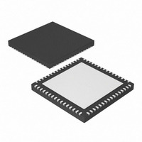
PIC24FJ256GB106-I/MR Microchip Technology, PIC24FJ256GB106-I/MR Datasheet - Page 200

PIC24FJ256GB106-I/MR
Manufacturer Part Number
PIC24FJ256GB106-I/MR
Description
IC, 16BIT MCU, PIC24F, 32MHZ, QFN-64
Manufacturer
Microchip Technology
Series
PIC® 24Fr
Datasheets
1.PIC24FJ128GA106-IPT.pdf
(52 pages)
2.PIC24FJ64GB106-IPT.pdf
(16 pages)
3.PIC24FJ64GB106-IPT.pdf
(352 pages)
4.PIC24FJ192GB108-IPT.pdf
(328 pages)
Specifications of PIC24FJ256GB106-I/MR
Controller Family/series
PIC24
No. Of I/o's
51
Ram Memory Size
16KB
Cpu Speed
32MHz
No. Of Timers
5
Core Size
16 Bit
Program Memory Size
256KB
Peripherals
ADC, Comparator, PWM, RTC, Timer
Core Processor
PIC
Speed
32MHz
Connectivity
I²C, SPI, UART/USART, USB OTG
Number Of I /o
51
Program Memory Type
FLASH
Ram Size
16K x 8
Voltage - Supply (vcc/vdd)
2 V ~ 3.6 V
Data Converters
A/D 16x10b
Oscillator Type
Internal
Operating Temperature
-40°C ~ 85°C
Package / Case
64-VFQFN, Exposed Pad
Processor Series
PIC24FJ
Core
PIC
Data Bus Width
16 bit
Data Ram Size
16 KB
Interface Type
I2C, SPI, UART
Maximum Clock Frequency
32 MHz
Number Of Programmable I/os
52
Number Of Timers
5
Maximum Operating Temperature
+ 85 C
Mounting Style
SMD/SMT
3rd Party Development Tools
52713-733, 52714-737, 53276-922, EWDSPIC
Development Tools By Supplier
PG164130, DV164035, DV244005, DV164005, PG164120, DM240001, DM240011
Minimum Operating Temperature
- 40 C
On-chip Adc
10 bit, 16 Channel
Lead Free Status / RoHS Status
Lead free / RoHS Compliant
For Use With
876-1004 - PIC24 BREAKOUT BOARD
Eeprom Size
-
Lead Free Status / Rohs Status
Details
Available stocks
Company
Part Number
Manufacturer
Quantity
Price
Company:
Part Number:
PIC24FJ256GB106-I/MR
Manufacturer:
TI
Quantity:
1 292
- PIC24FJ128GA106-IPT PDF datasheet
- PIC24FJ64GB106-IPT PDF datasheet #2
- PIC24FJ64GB106-IPT PDF datasheet #3
- PIC24FJ192GB108-IPT PDF datasheet #4
- Current page: 200 of 328
- Download datasheet (6Mb)
PIC24FJ256GB110 FAMILY
17.1.1
Because the buffers and their BDs are shared between
the CPU and the USB module, a simple semaphore
mechanism is used to distinguish which is allowed to
update the BD and associated buffers in memory. This
is done by using the UOWN bit as a semaphore to
distinguish which is allowed to update the BD and
associated buffers in memory. UOWN is the only bit
that is shared between the two configurations of
BDnSTAT.
When UOWN is clear, the BD entry is “owned” by the
microcontroller core. When the UOWN bit is set, the BD
entry and the buffer memory are “owned” by the USB
peripheral. The core should not modify the BD or its
corresponding data buffer during this time. Note that
the microcontroller core can still read BDnSTAT while
the SIE owns the buffer and vice versa.
The buffer descriptors have a different meaning based
on the source of the register update. Register 17-1 and
Register 17-2 show the differences in BDnSTAT
depending on its current “ownership”.
REGISTER 17-1:
DS39897B-page 198
bit 15
bit 7
Legend:
R = Readable bit
-n = Value at POR
bit 15
bit 14
bit 13-10
bit 9-0
UOWN
R/W-x
R/W-x
BC7
BUFFER OWNERSHIP
UOWN: USB Own bit
1 = The USB module owns the BD and its corresponding buffer; the CPU must not modify the BD or
DTS: Data Toggle Packet bit
1 = Data 1 packet
0 = Data 0 packet
PID3:PID0: Packet Identifier bits (written by the USB module)
In Device mode:
Represents the PID of the received token during the last transfer.
In Host mode:
Represents the last returned PID, or the transfer status indicator.
BC9:BC0: Byte Count
This represents the number of bytes to be transmitted or the maximum number of bytes to be received
during a transfer. Upon completion, the byte count is updated by the USB module with the actual
number of bytes transmitted or received.
R/W-x
R/W-x
DTS
BC6
the buffer
BDnSTAT: BUFFER DESCRIPTOR n STATUS REGISTER PROTOTYPE, USB
MODE (BD0STAT THROUGH BD63STAT)
W = Writable bit
‘1’ = Bit is set
R/W-x
R/W-x
PID3
BC5
R/W-x
R/W-x
PID2
BC4
Preliminary
U = Unimplemented bit, read as ‘0’
‘0’ = Bit is cleared
R/W-x
R/W-x
When UOWN is set, the user can no longer depend on
the values that were written to the BDs. From this point,
the USB module updates the BDs as necessary, over-
writing the original BD values. The BDnSTAT register is
updated by the SIE with the token PID and the transfer
count is updated.
17.1.2
The USB OTG module uses a dedicated DMA to
access both the BDT and the endpoint data buffers.
Since part of the address space of the DMA is dedi-
cated to the Buffer Descriptors, a portion of the memory
connected to the DMA must comprise a contiguous
address space properly mapped for the access by the
module.
PID1
BC3
DMA INTERFACE
R/W-x
R/W-x
PID0
BC2
© 2008 Microchip Technology Inc.
x = Bit is unknown
R/W-x
R/W-x
BC9
BC1
R/W-x
R/W-x
BC8
BC0
bit 8
bit 0
Related parts for PIC24FJ256GB106-I/MR
Image
Part Number
Description
Manufacturer
Datasheet
Request
R

Part Number:
Description:
Manufacturer:
Microchip Technology Inc.
Datasheet:

Part Number:
Description:
Manufacturer:
Microchip Technology Inc.
Datasheet:

Part Number:
Description:
Manufacturer:
Microchip Technology Inc.
Datasheet:

Part Number:
Description:
Manufacturer:
Microchip Technology Inc.
Datasheet:

Part Number:
Description:
Manufacturer:
Microchip Technology Inc.
Datasheet:

Part Number:
Description:
Manufacturer:
Microchip Technology Inc.
Datasheet:

Part Number:
Description:
Manufacturer:
Microchip Technology Inc.
Datasheet:

Part Number:
Description:
Manufacturer:
Microchip Technology Inc.
Datasheet:


