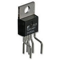
STR-W6253D Allegro Microsystems Inc, STR-W6253D Datasheet - Page 6

STR-W6253D
Manufacturer Part Number
STR-W6253D
Description
IC, AC-DC, REG, 6TO220
Manufacturer
Allegro Microsystems Inc
Datasheet
1.STR-W6253D.pdf
(15 pages)
Specifications of STR-W6253D
Output Current
-13µA
No. Of Outputs
1
Power Dissipation Pd
1.3W
Voltage Regulator Case Style
No. Of Pins
Operating Temperature Range
-20°C To +115°C
Package / Case
TO220
Base Number
6253
Output
RoHS Compliant
Input Voltage
17.1V
No. Of Pins
6
Rohs Compliant
Yes
Available stocks
Company
Part Number
Manufacturer
Quantity
Price
Company:
Part Number:
STR-W6253D
Manufacturer:
SANKEN
Quantity:
375
STR-W6253D
ELECTRICAL CHARACTERISTICS, continued, valid at V
Protection Operation
OCP Threshold Voltage at Zero
Duty Cycle (0% On-Duty)
Drain Peak Current Compensation
Coefficient
OCP Threshold Voltage After
Compensation
Leading Edge Blanking Time
OLP Delay Time
Circuit Current in OLP-Operation
OVP Protection Voltage
Latch Circuit Sustaining Current
Latch Circuit Release Voltage
ELP Threshold Voltage
Inflow Current at External Latch
Protection
Thermal Shut Down Operating
Temperature
Power MOSFET Characteristics
Drain-to-Source Breakdown Voltage
Drain Leakage Current
ON-Resistance
Switching Time
Thermal Resistance
Single Pulse Avalanche Energy
1
2
Input and output current polarity at the device pin; plus(+) represents sink and minus(–) represents source.
The latch circuit means a circuit operated ELP, OVP, and TSD.
Characteristic
2
2
V
Symbol Terminal
V
I
I
CC(La.OFF)
R
CC (OLP)
V
V
CC(La.H)
CC(OVP)
T
V
R
V
t
D
t
I
DS(ON)
I
E
blank
OCP1
OCP2
OLP
JTSD
DSS
ELP
DSS
ELP
θJ-F
t
PC
AS
r
3-5
3-5
1-5
1-5
4-5
4-5
4-5
4-5
7-5
7-5
1-3
1-3
1-3
1-3
–
–
–
–
60 W-Universal Input/90 W-230 Vac Input
Set V
terminal voltage level at which D/ST changes from
low to high) Measurement circuit 5
D
V
(The low portion of the D/ST terminal waveform at
V
(Time between setting FB terminal open and when
oscillation stops) Measurement circuit 6
(Inflow current into VCC terminal after OLP operation)
Measurement circuit 6
(VCC terminal voltage at which the voltage of D/ST
terminal is switched from low to high by decreasing
V
V
(Inflow current into VCC terminal after OVP operation)
Measurement circuit 1, V
(VCC voltage at which I
decreasing V
V
(FM/ELP terminal voltage at which the oscillation of
the D/ST terminal waveform is stopped by increasing
V
(Inflow current at V
I
V
I
Measurement circuit 9
Measured between junction and internal frame
Measurement circuit 11
D
D
OCP2
OCP
FB
CC
CC
FM
D
PC
= 300 μA, Measurement circuit 8
= 1.2 A, V
= 650 V, Measurement circuit 7
CC
) Measurement circuit 2
after setting V
= –0.75× SLP / f
= 18.0 V through 27 to 30 V
= 31.0 V through 7.8 to 6.4 V
= 2 V) Measurement circuit 5
FM
115 Northeast Cutoff, Box 15036
Allegro MicroSystems, Inc.
Worcester, Massachusetts 01615-0036 (508) 853-5000
www.allegromicro.com
= D
= 18 V, T
= 0 V and increase V
PC
FM
× D
CC
= 0 V Measurement circuit 10
after OVP operation)
MAX
A
Test Conditions
FM
= 25°C, unless otherwise specified
FM
+ V
OSC(av)
= 0 V) Measurement circuit 1,
= V
CC
OCP1
PWM Switching Regulators
CC
ELP
is dropped below 20 μA by
= 8 V
) Measurement circuit 2
OCP.
(V
OCP1
is the S/OCP
Min.
0.71
0.82
280
135
650
1.5
6.4
6.4
27
–
–
–
–
–
–
–
–
–
Typ.
0.78
0.93
28.5
400
200
410
140
1.9
7.1
7.1
55
–
–
–
–
–
–
–
Max
0.86
1.04
1.75
520
700
220
100
300
400
2.3
7.8
7.8
1.9
30
–
–
–
–
Units
DC%
°C/W
mV/
ms
ns
μA
μA
μA
°C
μA
ns
Ω
V
V
V
V
V
V
–
6


