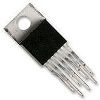
LM2588T-5.0 National Semiconductor, LM2588T-5.0 Datasheet - Page 25

LM2588T-5.0
Manufacturer Part Number
LM2588T-5.0
Description
IC, FLYBACK REGULATOR, TO-220-7
Manufacturer
National Semiconductor
Datasheet
1.LM2588S-ADJNOPB.pdf
(30 pages)
Specifications of LM2588T-5.0
Input Voltage
40V
Output Current
5A
Output Voltage
5V
No. Of Outputs
1
Supply Voltage Range
4V To 40V
No. Of Pins
7
Operating Temperature Range
-40°C To +125°C
Termination Type
Through Hole
Filter Terminals
Through Hole
Rohs Compliant
No
Lead Free Status / RoHS Status
Contains lead / RoHS non-compliant
Available stocks
Company
Part Number
Manufacturer
Quantity
Price
Company:
Part Number:
LM2588T-5.0/NOPB
Manufacturer:
RICHTEK
Quantity:
12 000
Company:
Part Number:
LM2588T-5.0/NOPB
Manufacturer:
National Semiconductor
Quantity:
135
Application Hints
FREQUENCY SYNCHRONIZATION
Another feature of the LM2588 is the ability to synchronize
the switching frequency to an external source, using the
sync pin (pin 6). This feature allows the user to parallel
multiple devices to deliver more output power.
A negative falling pulse applied to the sync pin will synchro-
nize the LM2588 to an external oscillator (see Figure 43 and
44).
Use of this feature enables the LM2588 to be synchronized
to an external oscillator, such as a system clock. This opera-
tion allows multiple power supplies to operate at the same
frequency, thus eliminating frequency-related noise prob-
lems.
The scope photo in Figure 44 shows a LM2588 12V Boost
Regulator synchronized to a 200 kHz signal. There is a 700
ns delay between the falling edge of the sync signal and the
turning on of the switch.
FIGURE 44. Waveforms of a Synchronized
12V Boost Regulator
(Continued)
FIGURE 45. Boost Regulator
01242064
25
PROGRAMMING OUTPUT VOLTAGE
(SELECTING R1 AND R2)
Referring to the adjustable regulator in Figure 45, the output
voltage is programmed by the resistors R1 and R2 by the
following formula:
Resistors R1 and R2 divide the output voltage down so that
it can be compared with the 1.23V internal reference. With
R2 between 1k and 5k, R1 is:
For best temperature coefficient and stability with time, use
1% metal film resistors.
SHORT CIRCUIT CONDITION
Due to the inherent nature of boost regulators, when the
output is shorted (see Figure 45 ), current flows directly from
the input, through the inductor and the diode, to the output,
bypassing the switch. The current limit of the switch does not
limit the output current for the entire circuit. To protect the
load and prevent damage to the switch, the current must be
externally limited, either by the input supply or at the output
with an external current limit circuit. The external limit should
be set to the maximum switch current of the device, which is
5A.
In a flyback regulator application (Figure 46 ), using the
standard transformers, the LM2588 will survive a short cir-
cuit to the main output. When the output voltage drops to
80% of its nominal value, the frequency will drop to 25 kHz.
With a lower frequency, off times are larger. With the longer
off times, the transformer can release all of its stored energy
before the switch turns back on. Hence, the switch turns on
initially with zero current at its collector. In this condition, the
switch current limit will limit the peak current, saving the
device.
V
R1 = R2 (V
OUT
= V
REF
OUT
(1 + R1/R2)
/V
REF
− 1)
01242056
where V
where V
REF
REF
www.national.com
= 1.23V
= 1.23V


