LM2733XMF National Semiconductor, LM2733XMF Datasheet - Page 3
LM2733XMF
Manufacturer Part Number
LM2733XMF
Description
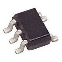
IC, BOOST CONVERTER, 5-SOT-23
Manufacturer
National Semiconductor
Datasheet
1.LM2733XMFNOPB.pdf
(14 pages)
Specifications of LM2733XMF
Primary Input Voltage
5V
No. Of Outputs
1
Output Voltage
40V
Output Current
1A
No. Of Pins
5
Operating Temperature Range
-40°C To +125°C
Peak Reflow Compatible (260 C)
No
Lead Free Status / RoHS Status
Contains lead / RoHS non-compliant
Available stocks
Company
Part Number
Manufacturer
Quantity
Price

Company:
Part Number:
LM2733XMF
Manufacturer:
MINI
Quantity:
5 000
Part Number:
LM2733XMF
Manufacturer:
NS/国半
Quantity:
20 000
Company:
Part Number:
LM2733XMF/NOPB
Manufacturer:
NS
Quantity:
3 000
Part Number:
LM2733XMF/NOPB
Manufacturer:
TI/德州仪器
Quantity:
20 000
Company:
Part Number:
LM2733XMFX
Manufacturer:
NS
Quantity:
5 321
Company:
Part Number:
LM2733XMFX
Manufacturer:
NS
Quantity:
1 453
Part Number:
LM2733XMFX
Manufacturer:
NS/国半
Quantity:
20 000
Part Number:
LM2733XMFX/NOPB
Manufacturer:
TI/德州仪器
Quantity:
20 000


V
I
R
SHDN
I
V
I
I
F
D
I
SW
SHDN
FB
Q
L
SW
IN
FB
DS
MAX
Symbol
Absolute Maximum Ratings
If Military/Aerospace specified devices are required,
please contact the National Semiconductor Sales Office/
Distributors for availability and specifications.
Electrical Characteristics
Limits in standard typeface are for T
(−40°C
Note 1: Absolute Maximum Ratings indicate limits beyond which damage to the component may occur. Electrical specifications do not apply when operating the
device outside of the limits set forth under the operating ratings which specify the intended range of operating conditions.
Note 2: The maximum power dissipation which can be safely dissipated for any application is a function of the maximum junction temperature, T
C, the junction-to-ambient thermal resistance for the SOT-23 package, θ
dissipation at any ambient temperature for designs using this device can be calculated using the formula:
If power dissipation exceeds the maximum specified above, the internal thermal protection circuitry will protect the device by reducing the output voltage as
required to maintain a safe junction temperature.
Note 3: The human body model is a 100 pF capacitor discharged through a 1.5 kΩ resistor into each pin. The machine model is a 200 pF capacitor discharged
directly into each pin.
Note 4: Limits are guaranteed by testing, statistical correlation, or design.
Note 5: Typical values are derived from the mean value of a large quantity of samples tested during characterization and represent the most likely expected value
of the parameter at room temperature.
Note 6: Switch current limit is dependent on duty cycle (see Typical Performance Characteristics). Limits shown are for duty cycles
Storage Temperature Range
Operating Junction
Lead Temp. (Soldering, 5 sec.)
Power Dissipation
(ON)
TH
Temperature Range
≤
T
J
Input Voltage
Switch Current Limit
Switch ON Resistance
Shutdown Threshold
Shutdown Pin Bias Current
Feedback Pin Reference
Voltage
Feedback Pin Bias Current
Quiescent Current
FB Voltage Line Regulation
Switching Frequency
Maximum Duty Cycle
Switch Leakage
≤
+125°C). Unless otherwise specified: V
(Note
Parameter
2)
J
= 25°C, and limits in boldface type apply over the full operating temperature range
−65°C to +150°C
−40°C to +125°C
Internally Limited
(Note
I
Device ON
Device OFF
V
V
V
V
V
V
V
V
2.7V
“X” Option
“Y” Option
“X” Option
“Y” Option
Not Switching V
SW
SHDN
SHDN
IN
FB
SHDN
SHDN
SHDN
SHDN
(Note
= 3V
= 100 mA
= 1.23V
≤
6)
= 0
= 5V
= 5V, Switching "X"
= 5V, Switching "Y"
= 5V, Not Switching
= 0
V
300°C
1)
IN
IN
Conditions
≤
= 5V, V
14V
J-A
SW
= 265°C/W, and the ambient temperature, T
3
SHDN
= 5V
FB Pin Voltage
SW Pin Voltage
Input Supply Voltage
SHDN Pin Voltage
θ
ESD Rating
= 5V, I
J-A
(SOT23-5)
Human Body Model
Machine Model
L
= 0A.
(Note
(Note
1.205
1.15
0.40
Min
2.7
1.0
1.5
87
93
4)
3)
(Note
Typical
1.230
0.024
0.02
0.60
500
400
1.5
2.1
1.1
1.6
60
93
96
A
0
0
. The maximum allowable power
5)
≤
(Note
−0.4V to VIN + 0.3V
1.255
50%.
Max
0.50
1.85
650
500
3.0
0.8
14
2
2
1
1
−0.4V to +14.5V
4)
−0.4V to +40V
−0.4V to +6V
www.national.com
J
(MAX) = 125°
265°C/W
Units
MHz
%/V
200V
mΩ
mA
µA
nA
µA
µA
2 kV
%
V
A
V
V
Related parts for LM2733XMF
Image
Part Number
Description
Manufacturer
Datasheet
Request
R

Part Number:
Description:
Manufacturer:
National Semiconductor
Datasheet:
Part Number:
Description:
National Semiconductor [8-Bit D/A Converter]
Manufacturer:
National Semiconductor
Datasheet:
Part Number:
Description:
National Semiconductor [Media Coprocessor]
Manufacturer:
National Semiconductor
Datasheet:
Part Number:
Description:
Digitally Controlled Tone and Volume Circuit with Stereo Audio Power Amplifier, Microphone Preamp Stage and National 3D Sound
Manufacturer:
National Semiconductor
Datasheet:
Part Number:
Description:
Digitally Controlled Tone and Volume Circuit with Stereo Audio Power Amplifier, Microphone Preamp Stage and National 3D Sound
Manufacturer:
National Semiconductor
Datasheet:
Part Number:
Description:
AC97 Rev 2 Codec with Sample Rate Conversion and National 3D Sound
Manufacturer:
National Semiconductor
Part Number:
Description:
Manufacturer:
National Semiconductor
Datasheet:
Part Number:
Description:
Manufacturer:
National Semiconductor
Datasheet:
Part Number:
Description:
General Purpose, Low Voltage, Low Power, Rail-to-Rail Output Operational Amplifiers
Manufacturer:
National Semiconductor
Datasheet:
Part Number:
Description:
8-bit 20 MSPS flash A/D converter.
Manufacturer:
National Semiconductor
Datasheet:
Part Number:
Description:
Low Noise Quad Operational Amplifier
Manufacturer:
National Semiconductor
Datasheet:
Part Number:
Description:
Quad Differential Line Receivers
Manufacturer:
National Semiconductor
Datasheet:
Part Number:
Description:
Quad High Speed Trapezoidal? Bus Transceiver
Manufacturer:
National Semiconductor
Datasheet:
Part Number:
Description:
Dual Line Receiver
Manufacturer:
National Semiconductor
Datasheet: