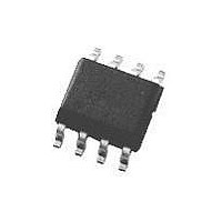
LM3488MM National Semiconductor, LM3488MM Datasheet - Page 14

LM3488MM
Manufacturer Part Number
LM3488MM
Description
IC, N-CH CONTROLLER, MSOP-8
Manufacturer
National Semiconductor
Datasheet
1.LM3488MM.pdf
(24 pages)
Specifications of LM3488MM
Primary Input Voltage
40V
No. Of Outputs
1
Output Current
1A
No. Of Pins
8
Operating Temperature Range
-40°C To +125°C
Termination Type
SMD
Input Voltage Primary Min
2.95V
Output Voltage Min
1.26V
Rohs Compliant
No
Lead Free Status / RoHS Status
Contains lead / RoHS non-compliant
Available stocks
Company
Part Number
Manufacturer
Quantity
Price
Part Number:
LM3488MM
Manufacturer:
NS/国半
Quantity:
20 000
Company:
Part Number:
LM3488MM/NOPB
Manufacturer:
TI
Quantity:
15 540
Part Number:
LM3488MMX
Manufacturer:
NS/国半
Quantity:
20 000
Company:
Part Number:
LM3488MMX/NOPB
Manufacturer:
ATMEL
Quantity:
3 410
www.national.com
Typical Applications
The LM3488 may be operated in either continuous or discon-
tinuous conduction mode. The following applications are de-
signed for continuous conduction operation. This mode of
operation has higher efficiency and lower EMI characteristics
than the discontinuous mode.
BOOST CONVERTER
The most common topology for LM3488 is the boost or step-
up topology. The boost converter converts a low input voltage
into a higher output voltage. The basic configuration for a
boost regulator is shown in
tion mode (when the inductor current never reaches zero at
steady state), the boost regulator operates in two cycles. In
the first cycle of operation, MOSFET Q is turned on and en-
ergy is stored in the inductor. During this cycle, diode D is
reverse biased and load current is supplied by the output ca-
pacitor, C
In the second cycle, MOSFET Q is off and the diode is forward
biased. The energy stored in the inductor is transferred to the
POWER INDUCTOR SELECTION
The inductor is one of the two energy storage elements in a
boost converter.
varies during a switching cycle. The current through an in-
ductor is quantified as:
FIGURE 10. Simplified Boost Converter Diagram (a) First cycle of operation. (b) Second cycle of operation
OUT
.
Figure 11
Figure
shows how the inductor current
10. In continuous conduc-
14
load and output capacitor. The ratio of these two cycles de-
termines the output voltage. The output voltage is defined as:
(ignoring the drop across the MOSFET and the diode), or
where D is the duty cycle of the switch, V
age drop of the diode, and V
when it is on. The following sections describe selection of
components for a boost converter.
Q
is the drop across the MOSFET
D
is the forward volt-
10138822


