LM2990T-5.0 National Semiconductor, LM2990T-5.0 Datasheet - Page 4
LM2990T-5.0
Manufacturer Part Number
LM2990T-5.0
Description
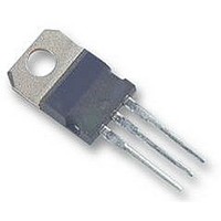
IC, V REG LDO -5.0V, 2990, TO-220-3
Manufacturer
National Semiconductor
Datasheet
1.LM2990T-5.0.pdf
(13 pages)
Specifications of LM2990T-5.0
Primary Input Voltage
-10V
Output Voltage
-5V
Dropout Voltage Vdo
600mV
No. Of Pins
3
Output Current
1A
Voltage Regulator Case Style
TO-220
Operating Temperature Range
-40°C To +125°C
Output Voltage Fixed
-5V
Rohs Compliant
Yes
Lead Free Status / RoHS Status
Lead free / RoHS Compliant
Available stocks
Company
Part Number
Manufacturer
Quantity
Price
Company:

Part Number:
LM2990T-5.0
Manufacturer:
NS
Quantity:
500
Company:
Part Number:
LM2990T-5.0
Manufacturer:
NS
Quantity:
353
Part Number:
LM2990T-5.0
Manufacturer:
NS/国半
Quantity:
20 000


www.national.com
Quiescent Current (I
Short Circuit Current
Maximum Output Current
Ripple Rejection
Output Noise Voltage
Long Term Stability
Electrical Characteristics
V
ing temperature range, −40˚C ≤ T
Note 1: Absolute Maximum Ratings indicate limits beyond which damage to the device may occur. Operating Ratings indicate conditions for which the device is
intended to be functional, but do not guarantee specific performance limits. For guaranteed specifications and test conditions, see the Electrical Characteristics.
Note 2: Human body model, 100 pF discharged through a 1.5 kΩ resistor.
Note 3: The maximum power dissipation is a function of T
− T
160˚C. For the LM2990, the junction-to-ambient thermal resistance, is 53˚C/W, 73˚C/W for the TO-263, and the junction-to-case thermal resistance is 3˚C. If the
TO-263 package is used, the thermal resistance can be reduced by increasing the P.C. board copper area thermally connected to the package. Using 0.5 square
inches of copper area, θ
Note 4: Typicals are at T
Note 5: Limits are guaranteed and 100% production tested.
Note 6: V
Note 7: The short circuit current is less than the maximum output current with the −12V and −15V versions due to internal foldback current limiting. The −5V and
−5.2V versions, tested with a lower input voltage, does not reach the foldback current limit and therefore conducts a higher short circuit current level. If the LM2990
output is pulled above ground, the maximum allowed current sunk back into the LM2990 is 1.5A.
Definition of Terms
Dropout Voltage: The input-output voltage differential at
which the circuit ceases to regulate against further reduction
in input voltage. Measured when the output voltage has
dropped 100 mV from the nominal value obtained at (V
5V) input, dropout voltage is dependent upon load current
and junction temperature.
Input Voltage: The DC voltage applied to the input terminals
with respect to ground.
Input-Output Differential: The voltage difference between
the unregulated input voltage and the regulated output volt-
age for which the regulator will operate.
Line Regulation: The change in output voltage for a change
in the input voltage. The measurement is made under con-
ditions of low dissipation or by using pulse techniques such
that the average chip temperature is not significantly af-
fected.
IN
A
)/θ
= −5V + V
JA
Parameter
. If this dissipation is exceeded, the die temperature will rise above 125˚C, and the LM2990 will eventually go into thermal shutdown at a T
O(NOM)
is the nominal (typical) regulator output voltage, −5V, −5.2V, −12V or −15V.
O(NOM)
q
JA
)
J
= 25˚C and represent the most likely parametric norm.
is 50˚C/W; with 1 square inch of copper area, θ
(Note 6) , I
I
I
R
(Note 7)
V
ƒ
10 Hz–100 kHz, I
1000 Hours
O
O
ripple
ripple
L
≤ 1A
= 1A, V
= 1Ω (Note 7)
O
J
= 1 kHz, I
= 1 V
= 1A, C
≤ 125˚C, all other limits apply for T
Conditions
IN
rms
= V
O
,
(Continued)
O
O(NOM)
= 47 µF, unless otherwise specified. Boldface limits apply over the entire operat-
O
Jmax
= 5 mA
= 5 mA
, θ
JA
, and T
O
A
+
JA
. The maximum allowable power dissipation at any ambient temperature is P
is 37˚C/W; and with 1.6 or more square inches of copper area, θ
4
(Note 4)
2000
Typ
500
1.2
1.8
52
1
9
Load Regulation: The change in output voltage for a
change in load current at constant chip temperature.
Long Term Stability: Output voltage stability under accelle-
rated life-test conditions after 1000 hours with maximum
rated voltage and junction temperature.
Output Noise Voltage: The rms AC voltage at the output,
with constant load and no input ripple, measured over a
specified frequency range.
Quiescent Current: That part of the positive input current
that does not contribute to the positive load current. The
regulator ground lead current.
Ripple Rejection: The ratio of the peak-to-peak input ripple
voltage to the peak-to-peak output ripple voltage.
Temperature Stability of V
output voltage for a thermal variation from room temperature
to either temperature extreme.
LM2990-12
J
= 25˚C.
(Note 5)
Limit
1500
0.9
1.4
50
42
5
(Note 4)
2000
Typ
600
1.0
1.8
52
1
9
LM2990-15
O
: The percentage change in
(Note 5)
Limit
1800
0.75
1.4
50
42
5
JA
J
of approximately
is 32˚C/W.
mA (max)
mA (max)
µV (max)
dB (min)
D
A (min)
A (min)
(Limit)
Units
= (T
ppm
Jmax
Related parts for LM2990T-5.0
Image
Part Number
Description
Manufacturer
Datasheet
Request
R

Part Number:
Description:
IC REGULATOR NEG LDO TO220-3
Manufacturer:
National Semiconductor
Datasheet:
Part Number:
Description:
IC REGULATOR NEG LDO TO220-3
Manufacturer:
National Semiconductor
Datasheet:
Part Number:
Description:
IC REGULATOR NEG LDO TO220-3
Manufacturer:
National Semiconductor
Datasheet:

Part Number:
Description:
Linear Voltage Regulator IC
Manufacturer:
National Semiconductor
Datasheet:
Part Number:
Description:
IC,VOLT REGULATOR,FIXED,-5.2V,BIPOLAR,SIP,3PIN,PLASTIC
Manufacturer:
National Semiconductor
Datasheet:
Part Number:
Description:
IC REGULATOR NEG LDO TO220-3
Manufacturer:
National Semiconductor
Datasheet:
Part Number:
Description:
Linear Voltage Regulator IC
Manufacturer:
National Semiconductor

Part Number:
Description:
Negative Low Dropout Regulator
Manufacturer:
National Semiconductor Corporation
Datasheet:
Part Number:
Description:
Lm2990qml Negative Low Dropout Regulator
Manufacturer:
National Semiconductor Corporation
Datasheet:
Part Number:
Description:
LM2900/LM3900/LM3301 Quad Amplifiers
Manufacturer:
National Semiconductor
Datasheet:
Part Number:
Description:
National Semiconductor [8-Bit D/A Converter]
Manufacturer:
National Semiconductor
Datasheet:
Part Number:
Description:
National Semiconductor [Media Coprocessor]
Manufacturer:
National Semiconductor
Datasheet:
Part Number:
Description:
Digitally Controlled Tone and Volume Circuit with Stereo Audio Power Amplifier, Microphone Preamp Stage and National 3D Sound
Manufacturer:
National Semiconductor
Datasheet:
Part Number:
Description:
Digitally Controlled Tone and Volume Circuit with Stereo Audio Power Amplifier, Microphone Preamp Stage and National 3D Sound
Manufacturer:
National Semiconductor
Datasheet: