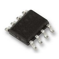
LP2997MR National Semiconductor, LP2997MR Datasheet - Page 9

LP2997MR
Manufacturer Part Number
LP2997MR
Description
IC, REG DDR TERMINATION, SMD, PSOP8
Manufacturer
National Semiconductor
Datasheet
1.LP2997MRNOPB.pdf
(12 pages)
Specifications of LP2997MR
Primary Input Voltage
2.5V
Output Voltage
0.957V
No. Of Pins
8
Output Current
500mA
Voltage Regulator Case Style
PSOP
Operating Temperature Range
0°C To +125°C
Svhc
No SVHC (15-Dec-2010)
Output Voltage Fixed
0.957V
Rohs Compliant
Yes
Lead Free Status / RoHS Status
Lead free / RoHS Compliant
Available stocks
Company
Part Number
Manufacturer
Quantity
Price
Part Number:
LP2997MR
Manufacturer:
TI/德州仪器
Quantity:
20 000
Company:
Part Number:
LP2997MR/NOPB
Manufacturer:
NS
Quantity:
285
Part Number:
LP2997MRX
Manufacturer:
NS/国半
Quantity:
20 000
Company:
Part Number:
LP2997MRX/NOPB
Manufacturer:
NS
Quantity:
11 650
Part Number:
LP2997MRX/NOPB
Manufacturer:
TI/德州仪器
Quantity:
20 000
Typical Application Circuits
Several different application circuits have been shown to il-
lustrate some of the options that are possible in configuring
the LP2997. Graphs of the individual circuit performance can
be found in the Typical Performance Characteristics section
in the beginning of the datasheet. These curves illustrate how
the maximum output current is affected by changes in AVIN
and PVIN.
Figure 2
DDR-II applications. The output stage is connected to the
1.8V rail and the AVIN pin can be connected to either a 2.5V,
3.3V or 5V rail.
PCB Layout Considerations
1.
2.
3.
4.
The input capacitor for the power rail should be placed
as close as possible to the PVIN pin.
V
at the point where regulation is required. For
motherboard applications an ideal location would be at
the center of the termination bus.
V
either the DIMM or the Chipset. This provides the most
accurate point for creating the reference voltage.
For improved thermal performance excessive top side
copper should be used to dissipate heat from the
SENSE
DDQ
shows the recommended circuit configuration for
can be connected remotely to the V
should be connected to the V
FIGURE 2. Recommended DDR-II Termination
TT
termination bus
DDQ
rail input at
9
This circuit permits termination in a minimum amount of board
space and component count. Capacitor selection can be var-
ied depending on the number of lines terminated and the
maximum load transient. However, with motherboards and
other applications where V
it is advisable to use multiple bulk capacitors and addition to
high frequency decoupling. The bulk output capacitors should
be situated at both ends of the V
ment. Large aluminum electrolytic capacitors are used for
their low ESR and low cost.
5.
6.
package. Numerous vias from the ground connection to
the internal ground plane will help. Additionally these can
be located underneath the package if manufacturing
standards permit.
Care should be taken when routing the V
avoid noise pickup from switching I/O signals. A 0.1uF
ceramic capacitor located close to the
used to filter any unwanted high frequency signal. This
can be an issue especially if long
V
ceramic capacitor for improved performance. This
capacitor should be located as close as possible to the
V
REF
REF
should be bypassed with a 0.01 µF or 0.1 µF
pin.
TT
is distributed across a long plane
20109413
TT
plane for optimal place-
SENSE
SENSE
traces are used.
SENSE
www.national.com
can also be
trace to


