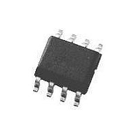
LP2986IMM-3.0 National Semiconductor, LP2986IMM-3.0 Datasheet - Page 7

LP2986IMM-3.0
Manufacturer Part Number
LP2986IMM-3.0
Description
IC, LDO VOLT REG, 3V, 0.2A, N8-SOIC
Manufacturer
National Semiconductor
Specifications of LP2986IMM-3.0
Primary Input Voltage
16V
Output Voltage Fixed
3V
Dropout Voltage Vdo
180mV
No. Of Pins
8
Output Current
200mA
Operating Temperature Range
-40°C To +125°C
Termination Type
SMD
Lead Free Status / RoHS Status
Contains lead / RoHS non-compliant
Available stocks
Company
Part Number
Manufacturer
Quantity
Price
Company:
Part Number:
LP2986IMM-3.0
Manufacturer:
NSC
Quantity:
200
Part Number:
LP2986IMM-3.0
Manufacturer:
NS/国半
Quantity:
20 000
Electrical Characteristics
Note 1: Absolute Maximum Ratings indicate limits beyond which damage to the component may occur. Electrical specifications do not apply when operating the
device outside of its rated operating conditions.
Note 2: The ESD rating of the Feedback pin is 500V. The ESD rating of the V
Note 3: The maximum allowable power dissipation is a function of the maximum junction temperature, T
and the ambient temperature, T
The value of θ
dependent on PCB trace area, trace material, and the number of layers and thermal vias. For improved thermal resistance and power dissipation for the LLP
package, refer to Application Note AN-1187. Exceeding the maximum allowable power dissipation will cause excessive die temperature, and the regulator will go into
thermal shutdown.
Note 4: If used in a dual-supply system where the regulator load is returned to a negative supply, the LM2986 output must be diode-clamped to ground.
Note 5: The output PNP structure contains a diode between the V
turn on this diode and may induce a latch-up mode which can damage the part (see Application Hints).
Note 6: Limits are 100% production tested at 25˚C. Limits over the operating temperature range are guaranteed through correlation using Statistical Quality Control
(SQC) methods. The limits are used to calculate National’s Average Outgoing Quality Level (AOQL).
Note 7: Dropout voltage is defined as the input to output differential at which the output voltage drops 100 mV below the value measured with a 1V differential.
Note 8: To prevent mis-operation, the Shutdown input must be driven by a signal that swings above V
Application Hints).
Note 9: Temperature coefficient is defined as the maximum (worst-case) change divided by the total temperature range.
Note 10: V
Note 11: See Typical Performance Characteristics curves.
FB
J−A
≤ V
OUT
for the SO-8 (M) package is 160˚C/W, and the mini SO-8 (MM) package is 200˚C/W. The value θ
≤ (V
IN
− 1), 2.5V ≤ V
A
. The maximum allowable power dissipation at any ambient temperature is calculated using:
IN
≤ 16V, 100 µA ≤ I
(Continued)
L
≤ 200 mA, T
IN
and V
OUT
J
IN
≤ 125˚C.
7
terminals that is normally reverse-biased. Forcing the output above the input will
pin is 1kV and the Tap pin is 1.5 kV.
H
and below V
J
(MAX), the junction-to-ambient thermal resistance, θ
L
J−A
with a slew rate not less than 40 mV/µs (see
for the LLP (LD) package is specifically
www.national.com
J−A
,


