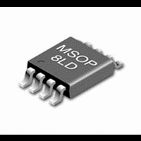
SI91821DH-AD-T1 Vishay, SI91821DH-AD-T1 Datasheet - Page 6

SI91821DH-AD-T1
Manufacturer Part Number
SI91821DH-AD-T1
Description
IC, ADJ LDO REG, 1.5V TO 5V, 0.3A, MSOP8
Manufacturer
Vishay
Datasheet
1.SI91821DH-277-T1.pdf
(11 pages)
Specifications of SI91821DH-AD-T1
Primary Input Voltage
6V
Output Voltage Adjustable Range
1.5V To 5V
Dropout Voltage Vdo
120mV
No. Of Pins
8
Output Current
300mA
Operating Temperature Range
-40°C To +85°C
Number Of Outputs
1
Polarity
Positive
Input Voltage Max
6 V
Output Voltage
1.5 V to 5 V
Output Type
Adjustable
Dropout Voltage (max)
0.02 V at 10 mA
Line Regulation
10 mV
Load Regulation
30 mV
Voltage Regulation Accuracy
1.5 %
Maximum Power Dissipation
0.666 W
Maximum Operating Temperature
+ 85 C
Mounting Style
SMD/SMT
Package / Case
MSOP-8
Minimum Operating Temperature
- 40 C
Lead Free Status / RoHS Status
Contains lead / RoHS non-compliant
Si91821
Vishay Siliconix
DETAILED DESCRIPTION
The Si91821 is a low drop out, low quiescent current, and very
linear regulator with very fast transient response. It is primarily
designed for battery powered applications where battery run
time is at a premium. The low quiescent current allows
extended standby time while low drop out voltage enables the
system to fully utilize battery power before recharge. The
Si91821 is a very fast regulator with bandwidth exceeding
50 kHz while maintaining low quiescent current at light load
conditions. With this bandwidth, the Si91821 is the fastest
LDO available today. The Si91821 is stable with any output
capacitor type from 1 mF to 10.0 mF. However, X5R or X7R
ceramic capacitors are recommended for best output noise
and transient performance.
V
V
is not critical as long as the input supply has low enough source
impedance. For practical circuits, a 1.0-mF or larger ceramic
capacitor is recommended. When the source impedance is
not low enough and/or the source is several inches from the
Si91821, then a larger input bypass capacitor is needed. It is
required that the equivalent impedance (source impedance,
wire, and trace impedance in parallel with input bypass
capacitor impedance) must be smaller than the input
impedance of the Si91821 for stable operation. When the
source impedance, wire, and trace impedance are unknown,
it is recommended that an input bypass capacitor be used of
a value that is equal to or greater than the output capacitor.
V
V
capacitor from V
any value from 1.0 mF to 10.0 mF. A ceramic capacitor with
X5R or X7R dielectric type is recommended for best output
noise, line transient, and load transient performance.
GND
Ground is the common ground connection for V
It is also the local ground connection for C
www.vishay.com
6
IN
IN
OUT
OUT
is the input supply pin. The bypass capacitor for this pin
is the output voltage of the regulator. Connect a bypass
OUT
to ground. The output capacitor can be
NOISE
, SET, and SD.
IN
and V
OUT
.
SET
SET is not connected internally for the fixed voltage version.
Therefore, it can be connected to GND optionally. For the
adjustable output version, use a resistor divider R
connect R
should be in the 25-kW to 150-kW range for low power
consumption, while maintaining adequate noise immunity.
The formula below calculates the value of R
desired output voltage and the R
SHUTDOWN (SD)
SD controls the turning on and off of the Si91821. V
guaranteed to be on when the SD pin voltage equals or is
greater than 1.5 V. V
pin voltage equals or is less than 0.4 V. During shutdown
mode, the Si91821 will draw less than 2-mA current from the
source. To automatically turn on V
applied, tie the SD pin to V
ERROR
ERROR is an open drain output that goes low when V
less than 5% of its normal value. As with any open drain output,
an external pull up resistor is needed. This function is active
in shutdown.
The ERROR pin must be left opened if not used.
C
For low noise application, connect a high frequency ceramic
capacitor from C
or X7R is recommended.
NOISE
R
V
1 +
SET
V
is nominally 1.215 V.
1
OUT
from V
V
* V
SET
NOISE
OUT
SET
OUT
to SET and R
R
to ground. A 0.01-mF or a 0.1-mF X5R
2
is guaranteed to be off when the SD
IN
.
2
value.
OUT
2
from SET to ground. R
S-51147–Rev. E, 20-Jun-05
whenever the input is
Document Number: 71614
1
, given the
1
and R
(1)
OUT
OUT
2
is
is
2
,


