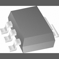
LM2937IMP-3.3 National Semiconductor, LM2937IMP-3.3 Datasheet - Page 4

LM2937IMP-3.3
Manufacturer Part Number
LM2937IMP-3.3
Description
IC, LDO REGULATOR, 3.3V, 0.5A, SOT223-3
Manufacturer
National Semiconductor
Datasheet
1.LM2937IMP-5.0NOPB.pdf
(13 pages)
Specifications of LM2937IMP-3.3
Primary Input Voltage
8.3V
Output Voltage Fixed
3.3V
No. Of Outputs
1
No. Of Pins
3
Output Current
500mA
Operating Temperature Range
-40°C To +85°C
Termination Type
SMD
Filter Terminals
SMD
Rohs Compliant
No
Lead Free Status / RoHS Status
Contains lead / RoHS non-compliant
Available stocks
Company
Part Number
Manufacturer
Quantity
Price
Company:
Part Number:
LM2937IMP-3.3
Manufacturer:
NS
Quantity:
10 000
Company:
Part Number:
LM2937IMP-3.3/NOPB
Manufacturer:
National Semiconductor
Quantity:
34 883
Part Number:
LM2937IMP-3.3/NOPB
Manufacturer:
NS/国半
Quantity:
20 000
www.national.com
Output Voltage
Line Regulation
Load Regulation
Quiescent Current
Output Noise
Voltage
Long Term Stability
Dropout Voltage
Short-Circuit Current
Peak Line Transient
Voltage
Maximum Operational
Input Voltage
Reverse DC
Input Voltage
Reverse Transient
Input Voltage
Electrical Characteristics
V
age, C
indicted device., all other specifications are for T
Note 1: Absolute Maximum Ratings indicate limits beyond which damage to the device may occur. Electrical specifications do not apply when operating the device
outside of its rated Operating Conditions.
Note 2: The maximum allowable power dissipation at any ambient temperature is P
operation, T
125˚C and the electrical specifications do not apply. If the die temperature rises above 150˚C, the LM2937 will go into thermal shutdown. For the LM2937, the
junction-to-ambient thermal resistance θ
with a heatsink, θ
or SOT-223 packages are used, the thermal resistance can be reduced by increasing the P.C. board copper area thermally connected to the package (see
Application Hints for more information on heatsinking).
Note 3: ESD rating is based on the human body model, 100 pF discharged through 1.5 kΩ.
Note 4: Typicals are at T
IN
= V
OUT
Parameter
NOM
A
is the ambient temperature, and θ
= 10 µF unless otherwise indicated. Boldface limits apply over the entire operating temperature range of the
+ 5V, (Note 4) I
JA
is the sum of the LM2937 junction-to-case thermal resistance θ
Output Voltage (V
J
= 25˚C and represent the most likely parametric norm.
OUTmax
5 mA ≤ I
(V
I
5 mA ≤ I
(V
I
V
I
10 Hz–100 kHz,
I
1000 Hrs.
I
I
t
V
t
OUT
OUT
OUT
OUT
OUT
OUT
f
r
IN
OUT
JA
<
<
OUT
OUT
is 65˚C/W, for the TO-220 package, 73˚C/W for the TO-263 package, and 174˚C/W for the SOT-223 package. When used
= (V
100 ms, R
1 ms, R
= 5 mA
= 5 mA
= I
= 5 mA
= I
= 50 mA
≥ −0.6V, R
= 500 mA for the TO-220 and TO-263 packages, I
+ 2V) ≤ V
+ 2V) ≤ V
OUT
OUTmax
OUTmax
JA
OUT
OUT
OUT
Conditions
is the junction-to-ambient thermal resistance. If this dissipation is exceeded, the die temperature will rise above
)
L
+ 5V),
≤ I
≤ I
= 100Ω
L
OUTmax
OUTmax
IN
IN
= 100Ω
L
= 100Ω
≤ 26V,
≤ 26V,
A
= T
J
= 25˚C.
4
JC
12.00
Typ
360
110
−30
−75
0.5
1.0
of 3˚C/W and the heatsink case-to-ambient thermal resistance. If the TO-263
MAX
36
12
10
44
75
2
= (125 − T
12V
11.64
11.40
12.36
12.60
Limit
A
−15
−50
120
120
250
1.0
0.6
10
20
60
26
)/θ
JA
, where 125 is the maximum junction temperature for
OUTmax
15.00
Typ
450
110
−30
−75
0.5
1.0
=400mA for the SOT-223 pack-
45
15
10
56
75
2
15V
14.55
14.25
15.45
15.75
Limit
150
150
250
−15
−50
1.0
0.6
10
20
60
26
mV(Max)
mV(Max)
mA(Max)
mA(Max)
mV(Max)
V (Min)
V(Max)
V(Max)
V(Max)
V(Min)
A(Min)
V(Min)
V(Min)
V(Min)
V(Min)
µVrms
Units
mV


