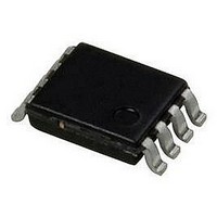
SC1104BISTRT Semtech, SC1104BISTRT Datasheet - Page 7

SC1104BISTRT
Manufacturer Part Number
SC1104BISTRT
Description
IC, VOLTAGE MODE PWM CTRL, 7V, 8-SOIC
Manufacturer
Semtech
Datasheet
1.SC1104AISTRT.pdf
(14 pages)
Specifications of SC1104BISTRT
Input Voltage
7V
Output Current
600mA
Frequency
600kHz
Supply Voltage Range
4.5V To 7V
Digital Ic Case Style
SOIC
No. Of Pins
8
Operating Temperature Range
-40°C To +85°C
Lead Free Status / RoHS Status
Lead free / RoHS Compliant
When choosing OC trip point one should consider the
Tempco of the MOSFETs Rds_on and SC1104’s Vtrip.
Also, any ringing on the Vcc and Phase nodes due to
parasitic L and C will have some effect on the OC Vtrip.
Example:
Iout_nom = 6A; assume I_max = 125% • Iout_nom =
7.5A
Rds_on = 0.014 ; assume Rds_on_max
Rds_on = 0.02
Voc = 7.5A • 0.02
This proves that MOSFETs with R
is the right choice.
Soft Start
The soft start (or hiccup) circuitry is activated when a
fault occurs. Faults occur for three reasons:
1) Under voltage (V
2) Over temperature (die temperature > 150°C)
3) Over current in high side FET.
All faults are handled the same way. Both DH and DL are
forced low. The error amplifier is turned off, but a 2µA
current flows into the comp pin (soft start current). The
sink current reduces the Comp voltage down to 0.6V
over a period of a few milliseconds. When Vcomp ~ 0.6V,
the fault is cleared and the DL goes high. Also, the soft
start current changes polarity and begins to increase the
voltage on the Comp capacitor. The DH remains low, be-
cause Vcomp is less than the lowest excursion of the
oscillator ramp (1.0V). After a few ms, the Vcomp in-
creases to about 1.0V and the DH will start to switch.
The duty cycle will gradually increase, and Vsns will in-
crease. When Vsns ~ 1.00V, the error amplifier turns on
again. The circuit has now reached its operating point. If
a fault occurs during the soft start, the cycle will begin
again (drivers low, Vcomp decreasing down to 0.6V).
Theory of Operation (Cont.)
©
POWER MANAGEMENT
2006 Semtech Corp.
CC
= 150mV.
< 4.2V)
DS_ON
= 0.014
150% •
@
25°C
7
Closing the Loop
In order to have a stable closed loop system with optimum
transient response one should make sure that open-loop
frequency response has an adequate Gain & Phase
margins. The Bode plot of log. Gain vs Freq. and Phase
vs Freq. provide the necessary means for the circuit
evaluation. Loop stability defined by compensation
networks around transconductance error amplifier (EA)
and output divider, see below and output capacitor Cout
and inductor Lout.
The inductor and output capacitor form a “double pole”
at the frequency:
The ESR of the output capacitor and the output capacitor
value create a “zero” at the frequency.
The “zero” and “pole” from the EA compensation network
are:
The additional “lead” network R
improve phase margin in case when output capacitors
with extra-low ESR are used and there is a need to
compensate for “high quality” output Lo, Co filter.
C
R
f
C
C
Z
Typical transconductance error amplifier
2
Cp
f
1
Rc
ESR
f
LC
EA
Gm
Cc
2
2
_
+
Cn
ESR
1
Rn
1
Vref
Lo
f
P
A
, C
SC1104A/B
Co
N
2
Co
, R
Ra
Rb
N
can be used to
www.semtech.com
1
Rc
Vout
Cp


