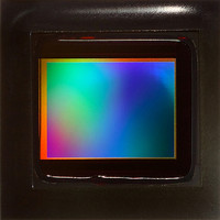
MT9P031I12STC Aptina LLC, MT9P031I12STC Datasheet - Page 4

MT9P031I12STC
Manufacturer Part Number
MT9P031I12STC
Description
IC, IMAGE SENSOR, 2.2 X 2.2µM, ILCC-48
Manufacturer
Aptina LLC
Type
CMOS Imagingr
Datasheets
1.MT9P031I12STCH_ES.pdf
(6 pages)
2.MT9P031I12STCH_ES.pdf
(12 pages)
3.MT9P031I12STCH_ES.pdf
(2 pages)
Specifications of MT9P031I12STC
Active Pixel Size
2592 X 1944
Pixel Size (h X W)
2.2 X 2.2
Frame Rate Per Sec
15
Color
RGB
Sensor Case Style
LCC
No. Of Pins
48
Supply Voltage Range
1.7V To 3.1V
Pixel Size
2.2µm x 2.2µm
Active Pixel Array
2592H x 1944V
Frames Per Second
60
Voltage - Supply
2.6 V ~ 3.1 V
Package / Case
48-iLCC
Rohs Compliant
Yes
Lead Free Status / RoHS Status
Lead free / RoHS Compliant
For Use With
557-1260 - KIT HEAD BOARD FOR MT9P031557-1258 - KIT DEV FOR MT9P031
Lead Free Status / RoHS Status
Lead free / RoHS Compliant, Lead free / RoHS Compliant
Other names
557-1262
MT9P031I12STC
Q3873226
MT9P031I12STC
Q3873226
Available stocks
Company
Part Number
Manufacturer
Quantity
Price
Company:
Part Number:
MT9P031I12STC
Manufacturer:
APTINA
Quantity:
1 000
Company:
Part Number:
MT9P031I12STC
Manufacturer:
APTINA
Quantity:
8 555
Part Number:
MT9P031I12STC
Manufacturer:
APTINA
Quantity:
20 000
Company:
Part Number:
MT9P031I12STCES
Manufacturer:
ProMOS
Quantity:
346
Company:
Part Number:
MT9P031I12STCH ES
Manufacturer:
Aptina LLC
Quantity:
135
Functional Overview
Figure 3:
PDF: 09005aef824c993e/Source: 09005aef824c9943
MT9P031_5100_PB_2.fm - Rev. B 8/07 EN
MT9P031 Block Diagram
The MT9P031 is a progressive-scan sensor that generates a stream of pixel data at a con-
stant frame rate. It uses an on-chip, phase-locked loop (PLL) to generate all internal
clocks from a single master input clock running between 6 MHz and 27 MHz. The maxi-
mum pixel rate is 96 megapixels per second, corresponding to a clock rate of 96 MHz.
Figure 3 illustrates a block diagram of the sensor.
STANDBY#
The sensor is programmed via the two-wire serial bus, which communicates with the
array control, analog signal chain, and digital signal chain. The core of the sensor is a 5-
megapixel active-pixel array. The timing and control circuitry sequences through the
rows of the array, resetting and then reading each row in turn. In the time interval
between resetting a row and reading that row, the pixels in the row integrate incident
light. The exposure is controlled by varying the time interval between reset and readout.
Once a row has been read, the data from the columns are sequenced through an analog
signal chain (providing offset correction and gain) and then through an ADC. The out-
put from the ADC is a 12-bit value for each pixel in the array. The ADC output passes
through a digital processing signal chain (which provides further data path corrections
and applies digital gain). The pixel data are output at a rate of up to 96 Mp/s, in addition
to frame and line synchronization signals.
TRIGGER
EXTCLK
RESET#
OE#
Analog Signal Chain
2,752H x 2,004V
Pixel Array
MT9P031: 1/2.5-Inch 5-Mp Digital Image Sensor
4
Micron Technology, Inc., reserves the right to change products or specifications without notice.
Data Path
Interface
Serial
Functional Overview
©2006 Micron Technology, Inc. All rights reserved.
SCLK
S
S
PIXCLK
D
LINE_VALID
FRAME_VALID
STROBE
DATA
ADDR
OUT
[11:0]


