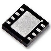
LM57BISD-5/NOPB National Semiconductor, LM57BISD-5/NOPB Datasheet - Page 13

LM57BISD-5/NOPB
Manufacturer Part Number
LM57BISD-5/NOPB
Description
IC, TEMPERATURE SW/SENSOR, ± 0.7°C, LLP8
Manufacturer
National Semiconductor
Datasheet
1.LM57BISD-10NOPB.pdf
(20 pages)
Specifications of LM57BISD-5/NOPB
Ic Output Type
Voltage
Sensing Accuracy Range
± 0.7°C
Supply Current
24µA
Supply Voltage Range
2.4V To 5.5V
Sensor Case Style
LLP
No. Of Pins
8
Msl
MSL 3 - 168 Hours
Accuracy %
0.8°C
Rohs Compliant
Yes
Lead Free Status / RoHS Status
Lead free / RoHS Compliant
3.0 T
The T
tive Low, Open-Drain Output both assert at the same time
whenever the Die Temperature reaches the Trip Point. They
also assert simultaneously whenever the TRIP TEST pin is
set high. Both outputs de-assert when the die temperature
goes below the (Temperature Trip Point) - (Hysteresis).
These two types of digital outputs enable the user the flexi-
bility to choose the type of output that is most suitable for his
design.
Either the T
open if not used.
The T
quires a pull-up resistor between this pin and V
3.1T
The LM57 has some noise immunity to a premature trigger
due to noise on the power supply. With the die temperature
at 1°C below the trip point, there are no premature triggers for
a square wave injected into the power supply with a magni-
tude of 100 mV
Above the frequency a premature trigger may occur.
With the die temperature at 2°C below the trip point, and a
magnitude of 200 mV
100 Hz to 300 kHz. Above that frequency a premature trigger
may occur.
Therefore if the supply line is noisy, it is recommended that a
local supply decoupling cap be used to reduce that noise.
4.0 TRIP TEST DIGITAL INPUT
The TRIP TEST pin provides a means to test the digital out-
puts by causing them to assert, regardless of temperature.
In addition, when the TRIP TEST pin is pulled high the
V
5.0 V
The V
source significant current. This is beneficial when, for exam-
ple, driving dynamic loads like an input stage on an analog-
to-digital converter (ADC). In these applications the source
current is required to quickly charge the input capacitor of the
ADC. See the Applications Circuits section for more discus-
sion of this topic. The LM57 is ideal for this and other appli-
cations which require strong source or sink current.
5.1 V
A load capacitor on V
For noisy environments, a 100nF supply decoupling cap
placed closed across V
mended.
5.2 V
The V
tremely noisy environment, or when driving a switched sam-
pling input on an ADC, it may be necessary to add some
filtering to minimize noise coupling. Without any precautions,
the V
1100 pF as shown in
than 1100 pF, a series resistor is required on the output, as
shown in
TEMP
OVER
OVER
TEMP
TEMP
TEMP
TEMP
OVER
OVER
TEMP
TEMP
pin will be at the V
Figure
and T
AND T
ANALOG TEMPERATURE SENSOR OUTPUT
Noise Considerations
Capacitive Loads
can drive a capacitive load less than or equal to
Active Low, Open-Drain Digital Output, if used, re-
Active High, Push-Pull Output and the T
Output handles capacitive loading well. In an ex-
push-pull output provides the ability to sink and
OVER
PP
OVER
3, to maintain stable conditions.
or the T
OVER
over a frequency range of 100 Hz to 2 MHz.
Noise Immunity
PP
TEMP
Figure
DIGITAL OUTPUTS
, there are no premature triggers from
DD
OVER
TRIP
can help to filter noise.
and GND pins of LM57 is recom-
2. For capacitive loads greater
voltage.
Digital Output pins can be left
DD
.
OVER
Ac-
13
5.3 V
The LM57 is very linear over temperature and supply voltage
range. Due to the intrinsic behavior of an NMOS/PMOS rail-
to-rail buffer, a slight shift in the output can occur when the
supply voltage is ramped over the operating range of the de-
vice. The location of the shift is determined by the relative
levels of V
V
This slight shift (a few millivolts) takes place over a wide
change (approximately 200 mV) in V
shift takes place over a wide temperature change of 5°C to
20°C, V
tions in the Electrical Characteristics table already includes
this possible shift.
6.0 MOUNTING AND TEMPERATURE CONDUCTIVITY
The LM57 can be applied easily in the same way as other
integrated-circuit temperature sensors. It can be glued or ce-
mented to a surface.
To ensure good temperature conductivity, the backside of the
LM57 die is directly attached to the exposed pad. The tem-
peratures of the lands and traces to the other leads of the
LM57 will also affect the temperature reading.
Alternatively, the LM57 can be mounted inside a sealed-end
metal tube, and can then be dipped into a bath or screwed
into a threaded hole in a tank. As with any IC, the LM57 and
accompanying wiring and circuits must be kept insulated and
dry, to avoid leakage and corrosion. This is especially true if
the circuit may operate at cold temperatures where conden-
sation can occur. If moisture creates a short circuit from the
DD
FIGURE 3. LM57 with Series Resistor for Capacitive
− V
FIGURE 2. LM57 No Isolation Resistor Required
TEMP
TEMP
TEMP
100 nF to 999 nF
Voltage Shift
1.1 nF to 99 nF
DD
= 1.0V.
is always monotonic. The accuracy specifica-
Loading greater than 1100 pF.
and V
C
1 μF
LOAD
TEMP
. The shift typically occurs when
Minimum R
1.5 kΩ
750 Ω
DD
3 kΩ
or V
30080516
TEMP
S
30080517
www.national.com
. Since the


