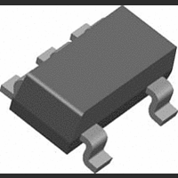
LM26CIM5-TPA National Semiconductor, LM26CIM5-TPA Datasheet - Page 5

LM26CIM5-TPA
Manufacturer Part Number
LM26CIM5-TPA
Description
IC, LOW POWER THERMOSTAT, ± 3°C, SOT23-5
Manufacturer
National Semiconductor
Datasheet
1.LM26CIM5-SHANOPB.pdf
(10 pages)
Specifications of LM26CIM5-TPA
Ic Output Type
Digital
Sensing Accuracy Range
± 3°C
Supply Current
16µA
Supply Voltage Range
2.7V To 5.5V
Sensor Case Style
SOT-23
No. Of Pins
5
Termination Type
SMD
Filter Terminals
SMD
Rohs Compliant
No
Lead Free Status / RoHS Status
Contains lead / RoHS non-compliant
Available stocks
Company
Part Number
Manufacturer
Quantity
Price
Part Number:
LM26CIM5-TPA
Manufacturer:
NS/国半
Quantity:
20 000
Company:
Part Number:
LM26CIM5-TPA/NOPB
Manufacturer:
ACX
Quantity:
1 422
Functional Description
LM26 OPTIONS
The LM26 can be factory programmed to have a trip point
anywhere in the range of −55°C to +110°C.
Applications Hints
AFTER-ASSEMBLY PCB TESTING
The LM26's V
by following a simple test procedure. Simply measuring the
V
sembled properly and that its temperature sensing circuitry is
functional. The V
that can be overdriven by 1.5mA. Therefore, one can simply
force the V
state, thereby verifying that the comparator and output cir-
cuitry function after assembly. Here is a sample test proce-
dure that can be used to test the LM26CIM5-TPA which has
an 85°C trip point.
1.
2.
TEMP
Turn on V
temperature reading of the LM26 using the equation:
or
Verify that the temperature measured in step one is
within (±3°C + error of reference temperature sensor) of
the ambient/board temperature. The ambient/board
temperature (reference temperature) should be
measured using an extremely accurate calibrated
temperature sensor.
V
output voltage will verify that the LM26 has been as-
O
= (−3.479×10
TEMP
TEMP
+
and measure V
voltage to cause the digital output to change
TEMP
output allows after-assembly PCB testing
−30)) + 1.8015V
output has very weak drive capability
−6
×(T−30)
LM26-_ _A
LM26-_ _C
TEMP
2
) + (−1.082×10
. Then calculate the
FIGURE 1. Output Pin Options Block Diagrams
−2
×(T
10132312
10132314
(1)
(2)
5
3.
4.
5.
V
The V
40 µA sink). So care should be taken when attaching circuitry
to this pin. Capacitive loading may cause the V
oscillate. Simply adding a resistor in series as shown in
2
value of the resistor follow the guidelines given in
same value resistor will work for either placement of the re-
sistor. If an additional capacitive load is placed directly on the
LM26 output, rather than across C
a factor of 10 smaller than C
TEMP
will prevent oscillations from occurring. To determine the
A.
B.
C. Observe that OS is now low.
D. Release the V
E.
A.
B.
C. When OS goes low, note the V
D. V
E.
A.
B.
TEMP
LOADING
Observe that OS is high.
Drive V
Observe that OS is now high.
Observe that OS is high.
Drive V
Calculate Ttrig using
Gradually raise V
V
Calculate T
TEMP
TEMP
output has very weak drive capability (1 µA source,
Trig = V
.
TEMP
TEMP
HYST
to ground.
voltage down gradually.
LM26-_ _B
LM26-_ _D
TEMP
TEMP
using
TEMP
at OS trigger (HIGH->LOW)
pin.
LOAD
Equation
Equation
until OS goes HIGH. Note
.
LOAD
, it should be at least
2.
TEMP
2.
voltage.
TEMP
10132313
Table
10132315
www.national.com
output to
Figure
1. The


