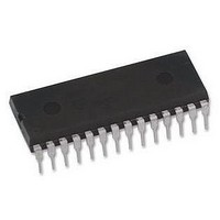
DG407DJ Vishay, DG407DJ Datasheet - Page 4

DG407DJ
Manufacturer Part Number
DG407DJ
Description
IC, MUX 8CH DP, DIP28, 407
Manufacturer
Vishay
Type
Analog Multiplexerr
Specifications of DG407DJ
No. Of Circuits
2
Supply Current
50µA
On State Resistance Max
50ohm
Supply Voltage Range
± 5V To ± 20V
Operating Temperature Range
-40°C To +85°C
Analogue Switch Case Style
DIP
No. Of Pins
28
Package
28PDIP
Maximum On Resistance
120@12V Ohm
Maximum Propagation Delay Bus To Bus
350@±15V ns
Maximum High Level Output Current
30 mA
Multiplexer Architecture
8:1
Maximum Turn-off Time
300@12V ns
Maximum Turn-on Time
600@12V ns
Power Supply Type
Single|Dual
Lead Free Status / RoHS Status
Lead free / RoHS Compliant
Available stocks
Company
Part Number
Manufacturer
Quantity
Price
Company:
Part Number:
DG407DJ
Manufacturer:
HARRIS
Quantity:
18
Company:
Part Number:
DG407DJ
Manufacturer:
MACOM
Quantity:
12 339
Part Number:
DG407DJ
Manufacturer:
INTERSIL
Quantity:
20 000
DG406/407
Vishay Siliconix
Notes:
a.
b.
c.
d.
e.
f.
g.
h.
www.vishay.com FaxBack 408-970-5600
5-4
Power Supplies
Positive Supply Current
Negative Supply Current
Positive Supply Current
Negative Supply Current
Analog Switch
Analog Signal Range
Drain-Source
On-Resistance
r
Channels
Source Off
Leakage Current
Drain Off
L
Leakage Current
Drain On
L
Leakage Current
Dynamic Characteristics
Switching Time of Multiplexer
Enable Turn-On Time
Enable Turn-Off Time
Charge Injection
Power Supplies
Positive Supply Current
Negative Supply Current
DS(on)
Refer to PROCESS OPTION FLOWCHART.
Room = 25 C, Full = as determined by the operating temperature suffix.
Typical values are for DESIGN AID ONLY, not guaranteed nor subject to production testing.
The algebraic convention whereby the most negative value is a minimum and the most positive a maximum, is used in this data sheet.
Guaranteed by design, not subject to production test.
V
Worst case isolation occurs on Channel 4 due to proximity to the drain pin.
k
k
IN
r
DS(on)
Matching Between
= input voltage to perform proper function.
Parameter
Parameter
C
C
g
= r
DS(on)
t
t
e
MAX – r
DS(on)
Symbol
Symbol
V
MIN.
t
t
t
OFF(EN)
ANALOG
r
ON(EN)
TRANS
I+
I–
I+
I–
DS(on)
r
I
I
I
I
I
S(off)
D(off)
D(off)
D(on)
D(on)
DS(on)
Q
I+
I–
Unless Otherwise Specified
S
Sequence Each Switch On
Unless Otherwise Specified
V
V
V
V
V
V
V
V
S1
EN
EN
D
S
S
V
V
S
Sequence Each Switch On
S
S
C
V
V+ = 15 V, V– = –15 V
AL
D
D
= 10 V or 0.5 V
= 0.5 V or 10 V
= 0.5 V or 10 V
= 8 V, V
V
Test Conditions
L
= 0 V or 5 V V
= 0 V or 5 V, V
V
V
= V
AL
V
Test Conditions
V
V
INH
INH
EN
EN
= 3 V, 10 V, I
= 1 nF, V
V
V+ = 12 V, V– = 0 V
10 V or 0 5 V
EN
EN
EN
EN
= 0.8 V, V
E
= 0.8 V, V
D
D
= 2.4 V, V
= 2.4 V, V
= 2.4 V, V
= 0 V
= V
= V
=
,
h S it h O
V
V
12 V V
S8
S1
A
A
E
10 V
= 0 V, V
S
= 0 or 5 V
= 0 or 5 V
= 5 V
= 6 V, R
,
AH
,
h S it h O
AH
5 V
A
A
S
S
A
A
INL
INL
= 2.4 V
= 0 V
= 0 V
= – 1 mA
= 0 V or 5 V
= 0 V or 5 V
= 2.4 V
0 V
IN
= 0 V
S
= 2.4 V
= 0
DG406
DG407
DG406
DG407
f
f
Temp
Temp
Room
Room
Room
Room
Room
Room
Room
Room
Room
Room
Room
Room
Room
Room
Room
Room
Room
Full
Full
Full
Full
Full
Full
Full
b
b
Typ
–0.01
–0.01
Typ
–0.01
13
50
0.01
0.04
0.04
0.04
0.04
300
250
150
90
20
13
5
c
c
Min
–10
–20
–20
–55 to 125 C
Min
–1
A Suffix
–20
–20
–55 to 125 C
0
A Suffix
d
d
Max
Max
500
900
30
75
120
450
600
300
12
30
75
d
d
S-00399—Rev. H, 13-Sep-99
Min
Min
Document Number: 70061
–10
–20
–20
–1
–20
–20
–40 to 85 C
–40 to 85 C
D Suffix
D Suffix
0
d
d
Max
Max
500
700
120
450
600
300
12
30
75
30
75
d
d
Unit
Unit
nA
nA
pC
ns
%
V
A
A
A
A
A
A


