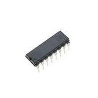
DG403DJ-E3 Vishay, DG403DJ-E3 Datasheet - Page 8

DG403DJ-E3
Manufacturer Part Number
DG403DJ-E3
Description
IC,ANALOG SWITCH,DUAL,SPDT,CMOS,DIP,16PIN,PLASTIC
Manufacturer
Vishay
Type
Analog Switchr
Datasheet
1.DG403DY-T1-E3.pdf
(12 pages)
Specifications of DG403DJ-E3
Rohs Compliant
YES
Number Of Switches
Dual
Switch Configuration
SPDT
On Resistance (max)
45 Ohms
On Time (max)
150 ns
Off Time (max)
100 ns
Supply Voltage (max)
25 V
Supply Current
0.00001 mA
Maximum Power Dissipation
450 mW
Maximum Operating Temperature
+ 85 C
Mounting Style
Through Hole
Package / Case
PDIP-16
Minimum Operating Temperature
- 40 C
Package
16PDIP
Maximum On Resistance
55@±13.5V Ohm
Maximum High Level Output Current
100 mA
Number Of Channels Per Chip
2
Maximum Turn-off Time
100@±15V ns
Maximum Turn-on Time
150@±15V ns
Switch Architecture
SPDT
Power Supply Type
Single|Dual
No. Of Channels
2
On State Resistance Max
45ohm
Turn Off Time
30ns
Turn On Time
75ns
Operating Temperature Range
-40°C To +85°C
Analog Switch Case Style
DIP
No. Of Pins
16
Analog Switch Type
SPDT
Lead Free Status / RoHS Status
Lead free / RoHS Compliant
Lead Free Status / RoHS Status
Lead free / RoHS Compliant
DG401, DG403, DG405
Vishay Siliconix
TEST CIRCUITS
V
trailing edge of the output waveform.
www.vishay.com
8
V
V
O
± 10 V
S1
S2
V
g
is the steady state output with the switch on. Feedthrough via switch capacitance may result in spikes at the leading and
+ 5 V
+ 5 V
S
S
IN
3 V
1
2
GND
R
C
V
S
IN
g
GND
L
L
V
(includes fixture and stray capacitance)
L
V
C
O
L
= V
(includes fixture and stray capacitance)
+ 15 V
+ 15 V
S
IN
+ 5 V
GND
S
V
L
- 15 V
- 15 V
V+
V-
V+
V-
D
D
D
1
2
R
L
R
+ r
L
+ 15 V
- 15 V
DS(on)
V+
V-
R
1
R
D
L
kΩ
L 2
L2
C
L2
V
O2
C
35 pF
L
10 nF
C
V
L
R
O
L1
Figure 3. Break-Before-Make
V
O
Figure 4. Charge Injection
Figure 2. Switching Time
C
L1
V
O1
Note: Logic input waveform is inverted for switches that
* V
S
Logic
Input
Switch
Switch
Output
Switch
Input*
Input*
= 10 V for t
have the opposite logic sense control
V
IN
O
Logic
Input
Switch
Output
Switch
Output
ON
-V
On
0 V
0 V
V
, V
S
S
S
V
V
V
V
3 V
0 V
0 V
0 V
= - 10 V for t
O1
O2
S1
S2
V
O
ΔV
O
50 %
Q = ΔV
OFF
90 %
Off
t
50 %
90 %
D
S09-2561-Rev. I, 30-Nov-09
t
ON
Document Number: 70049
O
x C
90 %
L
t
OFF
V
t
t
O
f
f
< 20 ns
< 20 ns
On
t
D
90 %


