DG428DN-E3 Vishay, DG428DN-E3 Datasheet - Page 3
DG428DN-E3
Manufacturer Part Number
DG428DN-E3
Description
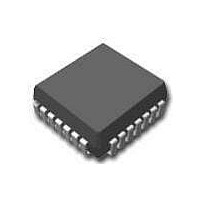
IC,ANALOG MUX,SINGLE,8-CHANNEL,CMOS,LDCC,20PIN,PLASTIC
Manufacturer
Vishay
Type
Analog Multiplexerr
Datasheet
1.DG428DN-E3.pdf
(12 pages)
Specifications of DG428DN-E3
Rohs Compliant
YES
Number Of Channels
8 Channel
On Resistance (max)
150 Ohms
Propagation Delay Time
250 ns
On Time (max)
300 ns
Off Time (max)
300 ns
Supply Voltage (max)
25 V
Supply Current
0.02 mA
Maximum Power Dissipation
800 mW
Maximum Operating Temperature
+ 85 C
Minimum Operating Temperature
- 40 C
Package / Case
PLCC-20
Mounting Style
SMD/SMT
Number Of Switches
Single
Package
20PLCC
Maximum On Resistance
150@12V Ohm
Maximum Propagation Delay Bus To Bus
250@±15V|280@12V ns
Maximum High Level Output Current
30 mA
Multiplexer Architecture
8:1
Maximum Turn-on Time
300@12V ns
Power Supply Type
Single|Dual
Lead Free Status / RoHS Status
Lead free / RoHS Compliant
Lead Free Status / RoHS Status
Lead free / RoHS Compliant
Available stocks
Company
Part Number
Manufacturer
Quantity
Price

Part Number:
DG428DN-E3
Manufacturer:
VISHAY/威世
Quantity:
20 000


Voltage Referenced to V–
V+
GND
Digital Inputs
Current (Any Terminal)
Peak Current, S or D
(Pulsed at 1 ms, 10% Duty Cycle Max)
Storage Temperature
Document Number: 70063
S-52433—Rev. J, 06-Sep-99
Analog Switch
Analog Signal Range
Drain-Source
On-Resistance
Greatest Change in r
Between Channels
Source Off
Leakage Current
Drain Off
L
Leakage Current
Drain On
L
Leakage Current
Digital Control
Logic Input Current
I
Input Voltage High
Logic Input Current
Input Voltage Low
Logic Input Capacitance
Dynamic Characteristics
Transition Time
Break-Before-Make Interval
Enable and Write
Turn-On Time
Enable and Reset
Turn-Off Time
Charge Injection
Off Isolation
Source Off Capacitance
Drain Off Capacitance
Drain Off Capacitance
Drain On Capacitance
Drain On Capacitance
. . . . . . . . . . . . . . . . . . . . . . . . . . . . . . . . . . . . . . . . . . . . . . . . . . . . . . . . . . .
g
k
k
t V lt
. . . . . . . . . . . . . . . . . . . . . . . . . . . . . . . . . . . . . . . . . . . . . . . . . . . . . . . . .
Parameter
p
C
C
a
, V
Hi h
S
t
t
, V
g
D
DS(on)
e
. . . . . . . . . . . . . . . . . . . . . . . .
. . . . . . . . . . . . . . . . . . . . . . . . . . . . . . . . . . . . . . .
(AK Suffix)
(DJ, DN Suffix)
t
Symbol
t
OFF(EN,RS)
ON(EN,WR)
V
t
r
ANALOG
C
C
C
C
C
TRANS
t
OIRR
DS(on)
I
I
I
I
I
r
OPEN
S(off)
D(off)
D(off)
D(on)
D(on)
DS(on)
I
I
C
I
S(off)
D(off)
D(off)
D(on)
D(on)
AH
AH
. . . . . . . . . . . . . . . . . . . . . . . .
AL
Q
in
. . . . . . . . . . . . . . . . . .
. . . . . . . . . . . . . .
30 mA, whichever occurs first
(V–) –2 V to (V+) +2 V or
Unless Otherwise Specified
V
V+ = 15 V, V– = –15 V, WR = 0,
V
V
EN
V
RS = 2.4 V, V
V
D
D
S
S
V
V
= 0 V, R
V
V
= 0 V, V
V
I
V
V
V
V
= 0 V, V
V
C
V
V
EN
S
= V
S
S
Test Conditions
D
V
GEN
f
f = 1 MHz
D
S
S
0 V V
EN
EN
AL
AH
See Figures 6 and 7
See Figures 6 and 8
L
RS = 0 V, WR = 0 V
= –1 mA, V
=
EN
–65 to 150 C
–10 V < V
= 7 V
–65 to 125 C
=
=
=
=
= 1 nF, See Figure 9
= 0 V, 2.4 V, V
D
1 MH
= 0.8 V
= 2.4 V
= 2.4 V
,
See Figure 5
See Figure 4
= 0 V
= 0 V, R
=
I
0 8 V
10 V, V
V
V
S
V
f = 1 MHz
10 V, V
L
10 V
10 V
10 V
EN
EN
RMS,
EN
A
EN
A
100 mA
= –1 mA
= 300
30 mA
= 2.4 V
10 V
= 15 V
IN
= 0 V
= 0 V, f = 1 MHz
44 V
25 V
= 0 V
0 V
S
= 2.4 V, 0.8 V
f = 100 kHz
AH
D
GEN
AL
< 10 V
=
= 2.4 V
= 0.8 V
A
C
= 0
= 0 V
L
10 V
= 15 pF
DG428
DG429
DG428
DG429
DG428
DG429
DG428
DG429
Power Dissipation (Package)
18-Pin Plastic DIP
18-Pin CerDIP
20-Pin PLCC
28-Pin Widebody SOIC
Notes:
a.
b.
c.
d.
e.
f.
f
Signals on S
diodes. Limit forward diode current to maximum current ratings.
All leads soldered or welded to PC board.
Derate 6.3 mW/ C above 75 C.
Derate 12 mW/ C above 75 C.
Derate 10 mW/ C above 75 C.
Derate 6 mW/ C above 75 C.
Temp
Room
Room
Room
Room
Room
Room
Room
Room
Room
Room
Room
Room
Room
Room
Room
Room
Room
Room
Full
Full
Full
Full
Full
Full
Full
Full
Full
Full
Full
Full
Full
Full
f
d
. . . . . . . . . . . . . . . . . . . . . . . . . . . . . . . . . . . . . . . . . . . . . .
. . . . . . . . . . . . . . . . . . . . . . . . . . . . . . . . . . . . . . . . . . . .
X
b
c
, D
. . . . . . . . . . . . . . . . . . . . . . . . . . . . . . . . . . . . . . . . .
X
Typ
f
or IN
–0.01
0.01
0.01
150
–75
55
30
90
55
40
20
54
34
0.03
0.07
0.05
0.07
0.05
11
. . . . . . . . . . . . . . . . . . . . . . . . . . . . . . . . . . . . .
5
8
1
c
X
b
exceeding V+ or V– will be clamped by internal
Min
–100
–100
–0.5
–15
–50
–50
–50
–55 to 125 C
–1
–1
–1
–1
–1
10
www.vishay.com FaxBack 408-970-5600
A Suffix
d
Vishay Siliconix
Max
100
125
100
100
250
300
150
225
150
300
0.5
15
50
50
50
1
1
1
1
1
1
d
DG428/429
Min
–100
–100
–0.5
–15
–50
–50
–50
–1
–1
–1
–1
–1
10
–40 to 85 C
D Suffix
d
Max
100
125
100
100
250
300
150
225
150
300
0.5
15
50
50
50
1
1
1
1
1
1
470 mW
900 mW
800 mW
450 mW
d
5-3
Unit
pC
nA
pF
dB
pF
ns
%
V
A
A
A
A
A
F
F
Related parts for DG428DN-E3
Image
Part Number
Description
Manufacturer
Datasheet
Request
R

Part Number:
Description:
IC, ANALOG MULTIPLEXER, 8 X 1, LCC-20
Manufacturer:
Vishay
Datasheet:
Part Number:
Description:
357-036-542-201 CARDEDGE 36POS DL .156 BLK LOPRO
Manufacturer:
Vishay
Datasheet:
Part Number:
Description:
357-036-542-201 CARDEDGE 36POS DL .156 BLK LOPRO
Manufacturer:
Vishay
Datasheet:
Part Number:
Description:
357-036-542-201 CARDEDGE 36POS DL .156 BLK LOPRO
Manufacturer:
Vishay
Datasheet:
Part Number:
Description:
357-036-542-201 CARDEDGE 36POS DL .156 BLK LOPRO
Manufacturer:
Vishay
Datasheet:
Part Number:
Description:
357-036-542-201 CARDEDGE 36POS DL .156 BLK LOPRO
Manufacturer:
Vishay
Datasheet:
Part Number:
Description:
357-036-542-201 CARDEDGE 36POS DL .156 BLK LOPRO
Manufacturer:
Vishay
Datasheet:
Part Number:
Description:
357-036-542-201 CARDEDGE 36POS DL .156 BLK LOPRO
Manufacturer:
Vishay
Datasheet:
Part Number:
Description:
357-036-542-201 CARDEDGE 36POS DL .156 BLK LOPRO
Manufacturer:
Vishay
Datasheet:
Part Number:
Description:
357-036-542-201 CARDEDGE 36POS DL .156 BLK LOPRO
Manufacturer:
Vishay
Datasheet:
Part Number:
Description:
357-036-542-201 CARDEDGE 36POS DL .156 BLK LOPRO
Manufacturer:
Vishay
Datasheet:
Part Number:
Description:
357-036-542-201 CARDEDGE 36POS DL .156 BLK LOPRO
Manufacturer:
Vishay
Datasheet:
Part Number:
Description:
357-036-542-201 CARDEDGE 36POS DL .156 BLK LOPRO
Manufacturer:
Vishay
Datasheet:
Part Number:
Description:
357-036-542-201 CARDEDGE 36POS DL .156 BLK LOPRO
Manufacturer:
Vishay
Datasheet:
Part Number:
Description:
357-036-542-201 CARDEDGE 36POS DL .156 BLK LOPRO
Manufacturer:
Vishay
Datasheet: