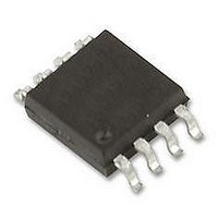
AD8566ARMZ Analog Devices Inc, AD8566ARMZ Datasheet - Page 9

AD8566ARMZ
Manufacturer Part Number
AD8566ARMZ
Description
AMP SENSOR PROG GAIN, 8566, MSOP8
Manufacturer
Analog Devices Inc
Datasheet
1.AD8566ARMZ.pdf
(12 pages)
Specifications of AD8566ARMZ
Op Amp Type
Rail To Rail
No. Of Amplifiers
2
Bandwidth
5MHz
Slew Rate
6V/µs
Supply Voltage Range
4.5V To 16V
Amplifier Case Style
MSOP
No. Of Pins
8
Operating Temperature Range
-40°C To
Lead Free Status / RoHS Status
Lead free / RoHS Compliant
Available stocks
Company
Part Number
Manufacturer
Quantity
Price
Company:
Part Number:
AD8566ARMZ
Manufacturer:
ADI
Quantity:
7 283
Part Number:
AD8566ARMZ
Manufacturer:
ADI/亚德诺
Quantity:
20 000
Company:
Part Number:
AD8566ARMZ-R2
Manufacturer:
AD
Quantity:
2 223
Part Number:
AD8566ARMZ-REEL
Manufacturer:
ADI/亚德诺
Quantity:
20 000
Part Number:
AD8566ARMZ-REEL7
Manufacturer:
ADI/亚德诺
Quantity:
20 000
REV. C
Output Phase Reversal
The AD856x family is immune to phase reversal. Although
the device’s output will not change phase, large currents due
to input overvoltage could damage the device. In applications
where the possibility of an input voltage exceeding the supply
voltage exists, overvoltage protection should be used as described
in the previous section.
Power Dissipation
The maximum allowable internal junction temperature of 150°C
limits the AD856x family’s maximum power dissipation of
AD856x devices. As the ambient temperature increases, the
maximum power dissipated by AD856x devices must decrease
linearly to maintain the maximum junction temperature. If this
maximum junction temperature is exceeded momentarily, the
device will still operate properly once the junction temperature is
reduced below 150°C. If the maximum junction temperature is
exceeded for an extended period of time, overheating could lead
to permanent damage of the device.
The maximum safe junction temperature, T
the following formula, we can obtain the maximum power that
an AD856x device can safely dissipate as a function of temperature:
where:
The power dissipated by the device can be calculated as
where:
Figure 3 shows the maximum power dissipation versus temperature.
To achieve proper operation, use the previous equation to calculate
P
figure below.
DISS
Figure 3. Maximum Power Dissipation vs. Temperature
for 5-, 8-, and 14-Lead Packages
P
T
T
θ
V
V
I
LOAD
J A
DISS
J MAX
A
S
OUT
= the ambient temperature of the circuit.
= the supply voltage.
for a specific package at any given temperature or use the
= the AD856x package thermal resistance,
1.25
1.00
0.75
0.50
0.25
= the AD856x power dissipation.
= the output voltage.
= the output load current.
junction-to-ambient.
= the AD856x maximum allowable junction
0
–35
temperature (150°C).
14-LEAD TSSOP
P
8-LEAD MSOP
5-LEAD SOT-23
14-LEAD SOIC
–15
DISS
P
DISS
= (V
AMBIENT TEMPERATURE ( C)
= T
5
S
– V
J MAX
25
OUT
– T
)
A
/ θ
45
I
J MAX
LOAD
J A
, is 150°C. Using
65
85
–9–
Total Harmonic Distortion + Noise (THD+N)
The AD856x family features low total harmonic distortion.
Figure 4 shows a graph of THD+N versus frequency. The THD+N
for the AD856x over the entire supply range is below 0.008%.
When the device is powered from a 16 V supply, the THD+N
stays below 0.003%. Figure 4 shows the AD8566 in a unity
noninverting configuration.
Short-Circuit Output Conditions
The AD856x family does not have internal short-circuit protection
circuitry. As a precautionary measure, it is recommended not to
short the output directly to the positive power supply or to ground.
It is not recommended to operate the AD856x with more than
35 mA of continuous output current. The output current can be
limited by placing a series resistor at the output of the amplifier
whose value can be derived using the following equation:
For a 5 V single-supply operation, R
value of 143 Ω.
LCD Panel Applications
The AD856x amplifier is designed for LCD panel applications
or applications where large capacitive load drive is required. It
can instantaneously source/sink greater than 250 mA of current.
At unity gain, it can drive 1 µF without compensation. This
makes the AD856x ideal for LCD V
To evaluate the performance of the AD856x family, a test circuit
was developed to simulate the V
LCD panel.
0.01
0.1
10
1
20
Figure 4. THD+N vs. Frequency Graph
100
AD8565/AD8566/AD8567
V
V
S
S
=
R
=
FREQUENCY (Hz)
X
2.5V
8V
≥
35 mA
COM
V
1k
S
X
COM
driver application for an
should have a minimum
driver applications.
10k
30k


