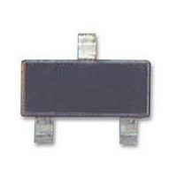
ADR5040ARTZ Analog Devices Inc, ADR5040ARTZ Datasheet - Page 11

ADR5040ARTZ
Manufacturer Part Number
ADR5040ARTZ
Description
IC, SM, SHUNT, VOLT REF, 2.048V
Manufacturer
Analog Devices Inc
Datasheet
1.ADR5041ARTZ-R2.pdf
(16 pages)
Specifications of ADR5040ARTZ
Topology
Shunt
Reference Voltage
2.048V
Reference Voltage Tolerance
4.096mV
Temperature Coefficient
100ppm/°C
Voltage Reference Case Style
SOT-23
No. Of Pins
3
Operating Temperature Range
-40°C
Lead Free Status / RoHS Status
Lead free / RoHS Compliant
Available stocks
Company
Part Number
Manufacturer
Quantity
Price
Company:
Part Number:
ADR5040ARTZ
Manufacturer:
Analog Devices Inc
Quantity:
25 199
Company:
Part Number:
ADR5040ARTZ-REEL7
Manufacturer:
AD
Quantity:
3 880
Part Number:
ADR5040ARTZ-REEL7
Manufacturer:
ADI/亚德诺
Quantity:
20 000
THEORY OF OPERATION
The ADR504x family uses the band gap concept to produce
a stable, low temperature coefficient voltage reference suitable
for high accuracy data acquisition components and systems. The
devices use the physical nature of a silicon transistor base-emitter
voltage in the forward-biased operating region. All such transistors
have approximately a −2 mV/°C temperature coefficient (TC),
making them unsuitable for direct use as a low temperature
coefficient reference. Extrapolation of the temperature charac-
teristic of any one of these devices to absolute zero (with the
collector current proportional to the absolute temperature),
however, reveals that its V
silicon band gap voltage. Therefore, if a voltage develops with
an opposing temperature coefficient to sum the V
temperature coefficient reference results.
APPLICATIONS INFORMATION
The ADR5040/ADR5041/ADR5043/ADR5044/ADR5045 are
a series of precision shunt voltage references. They are designed
to operate without an external capacitor between the positive
and negative terminals. If a bypass capacitor is used to filter the
supply, the references remain stable.
For a stable voltage, all shunt voltage references require an
external bias resistor (R
reference (see Figure 19). The R
through the load (I
and the supply voltage can vary, the R
based on the following considerations:
•
•
Given these conditions, R
voltage (V
ADR5045 load and operating current (I
ADR5040/ADR5041/ADR5043/ADR5044/ADR5045 output
voltage (V
R
to the ADR5040/ADR5041/ADR5043/ADR5044/ADR5045,
even when the supply voltage is at its minimum value and
the load current is at its maximum value.
R
when the supply voltage is at its maximum value and the
load current is at its minimum value.
R
BIAS
BIAS
BIAS
must be small enough to supply the minimum I
must be large enough so that I
OUT
S
), the ADR5040/ADR5041/ADR5043/ADR5044/
=
).
V
I
S
L
−
+
V
L
) and the reference (I
I
OUT
IN
BIAS
BIAS
BE
) between the supply voltage and the
approaches approximately the
is determined by the supply
BIAS
sets the current that flows
BIAS
IN
L
does not exceed 15 mA
and I
IN
needs to be chosen
). Because the load
IN
), and the
BE
, a zero
IN
current
Rev. A | Page 11 of 16
ADR5040/ADR5041/ADR5043/ADR5044/ADR5045
(3)
Precision Negative Voltage Reference
The ADR5040/ADR5041/ADR5043/ADR5044/ADR5045 are
suitable for applications where a precise negative voltage is desired.
Figure 20 shows the ADR5045 configured to provide a negative
output. Caution should be exercised in using a low temperature
sensitive resistor to avoid errors from the resistor.
Stacking the ADR504x for User-Definable Outputs
Multiple ADR504x parts can be stacked together to allow the
user to obtain a desired higher voltage. Figure 21a shows three
ADR5045 devices configured to give 15 V. The bias resistor,
R
flows through all the shunt references in series. Figure 21b shows
three ADR5045 devices stacked together to give −15 V. R
calculated in the same manner as before. Parts of different voltages
can also be added together; that is, an ADR5041 and an ADR5045
can be added together to give an output of +7.5 V or −7.5 V, as
desired. Note, however, that the initial accuracy error is the sum
of the errors of all the stacked parts, as are the temperature
coefficient and output voltage change vs. input current.
BIAS
, is chosen using Equation 3, noting that the same bias current
Figure 21. ±15 V Output with Stacked ADR5045 Devices
ADR5045
ADR5045
ADR5045
Figure 20. Negative Precision Reference Configuration
R
BIAS
R
I
IN
BIAS
V
(a)
DD
ADR5045
Figure 19. Shunt Reference
V
S
I
IN
ADR5040/ADR5041/
ADR5043/ADR5044/
ADR5045
+15V
R
I
+ I
L
BIAS
L
V
CC
ADR5045
ADR5045
ADR5045
V
OUT
R
BIAS
V
–5V
–V
OUT
(b)
DD
–15V
BIAS
is


