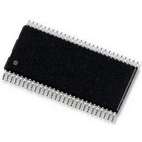
DS90CR287MTD National Semiconductor, DS90CR287MTD Datasheet

DS90CR287MTD
Specifications of DS90CR287MTD
Available stocks
Related parts for DS90CR287MTD
DS90CR287MTD Summary of contents
Page 1
... Gbit/s (297.5 Mbytes/sec). This chipset is an ideal means to solve EMI and cable size problems associated with wide, high-speed TTL interfaces. Block Diagrams DS90CR287 Order Number DS90CR287MTD See NS Package Number MTD56 © 2004 National Semiconductor Corporation Features MHz shift clock support n 50% duty cycle on receiver output clock n 2 Set & ...
Page 2
Pin Diagram for TSSOP Packages DS90CR287 Typical Application www.national.com 10108721 2 DS90CR288A 10108722 10108723 ...
Page 3
... Output TRI-STATE Current OZ LVDS RECEIVER DC SPECIFICATIONS V Differential Input High Threshold TH V Differential Input Low Threshold TL I Input Current IN (Note 1) Package Derating: DS90CR287MTD DS90CR288AMTD ESD Rating −0.3V to +4V (HBM, 1.5kΩ, 100pF) + 0.3V) (EIAJ, 0Ω, 200pF 0.3V) Latch Up Tolerance CC + 0.3V) +25˚ 0.3V) ...
Page 4
Electrical Characteristics Over recommended operating supply and temperature ranges unless otherwise specified Symbol Parameter TRANSMITTER SUPPLY CURRENT I Transmitter Supply Current Worst CCTW Case (with Loads) I Transmitter Supply Current Power CCTZ Down RECEIVER SUPPLY CURRENT I Receiver Supply Current ...
Page 5
Receiver Switching Characteristics Over recommended operating supply and temperature ranges unless otherwise specified Symbol CLHT CMOS/TTL Low-to-High Transition Time (Figure 3) CHLT CMOS/TTL High-to-Low Transition Time (Figure 3) RSPos0 Receiver Input Strobe Position for Bit 0 (Figure 15) RSPos1 Receiver ...
Page 6
AC Timing Diagrams FIGURE 2. DS90CR287 (Transmitter) LVDS Output Load and Transition Times FIGURE 3. DS90CR288A (Receiver) CMOS/TTL Output Load and Transition Times FIGURE 4. DS90CR287 (Transmitter) Input Clock Transition Time FIGURE 5. DS90CR287 (Transmitter) Setup/Hold and High/Low Times www.national.com ...
Page 7
AC Timing Diagrams (Continued) FIGURE 6. DS90CR288A (Receiver) Setup/Hold and High/Low Times FIGURE 7. DS90CR287 (Transmitter) Clock In to Clock Out Delay FIGURE 8. DS90CR288A (Receiver) Clock In to Clock Out Delay FIGURE 9. DS90CR287 (Transmitter) Phase Lock Loop Set ...
Page 8
AC Timing Diagrams FIGURE 10. DS90CR288A (Receiver) Phase Lock Loop Set Time FIGURE 11. 28 Parallel TTL Data Inputs Mapped to LVDS Outputs www.national.com (Continued) FIGURE 12. Transmitter Powerdown Delay 8 10108714 10108716 10108717 ...
Page 9
AC Timing Diagrams (Continued) FIGURE 14. Transmitter LVDS Output Pulse Position Measurement FIGURE 13. Receiver Powerdown Delay 9 10108718 10108719 www.national.com ...
Page 10
AC Timing Diagrams www.national.com (Continued) FIGURE 15. Receiver LVDS Input Strobe Position 10 10108728 ...
Page 11
AC Timing Diagrams C — Setup and Hold Time (Internal data sampling window) defined by Rspos (receiver input strobe position) min and max Tppos — Transmitter output pulse position (min and max) RSKM ≥ Cable Skew (type, length) + Source ...
Page 12
DS90CR288A MTD56 (TSSOP) Package Pin Description — Channel Link Receiver (Continued) Pin Name I/O No. GND I 5 Ground pins for TTL outputs. PLL Power supply for PLL. CC PLL GND I 2 Ground pin for PLL. ...
Page 13
Applications Information The TSSOP version of the DS90CR287 and DS90CR288A are backward compatible with the existing 5V Channel Link transmitter/receiver pair (DS90CR283, DS90CR284). To up- grade from 3.3V system the following must be addressed: 1. Change ...
Page 14
Applications Information ramic type in surface mount form factor) between each V and the ground plane(s) are recommended. The three ca- pacitor values are 0.1 µF, 0.01 µF and 0.001 µF. An example is shown in Figure 18. The designer ...
Page 15
Applications Information Input Clock section. Do not power up and enable (PWR DOWN = HIGH) the transmitter without a valid clock signal applied to the TxCLK IN pin. The CHANNEL LINK chipset is designed to protect itself from accidental loss ...
Page 16
... Physical Dimensions unless otherwise noted 56-Lead Molded Thin Shrink Small outline Package, JEDEC Order Number DS90CR287MTD or DS90CR288AMTD LIFE SUPPORT POLICY NATIONAL’S PRODUCTS ARE NOT AUTHORIZED FOR USE AS CRITICAL COMPONENTS IN LIFE SUPPORT DEVICES OR SYSTEMS WITHOUT THE EXPRESS WRITTEN APPROVAL OF THE PRESIDENT AND GENERAL COUNSEL OF NATIONAL SEMICONDUCTOR CORPORATION ...


