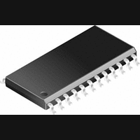
CS5508-BS Cirrus Logic Inc, CS5508-BS Datasheet - Page 27

CS5508-BS
Manufacturer Part Number
CS5508-BS
Description
A/D Converter (A-D) IC
Manufacturer
Cirrus Logic Inc
Datasheet
1.CS5508-BS.pdf
(40 pages)
Specifications of CS5508-BS
Peak Reflow Compatible (260 C)
No
Sample Rate
100 SPS
Supply Voltage Max
5V
No. Of Bits
20 Bit
Leaded Process Compatible
No
Mounting Type
Surface Mount
No. Of Channels
1
Power Rating
3.2mW
Lead Free Status / RoHS Status
Contains lead / RoHS non-compliant
Available stocks
Company
Part Number
Manufacturer
Quantity
Price
Part Number:
CS5508-BS
Manufacturer:
CIRRUS
Quantity:
20 000
Part Number:
CS5508-BSZ
Manufacturer:
CIRRUS
Quantity:
20 000
PIN DESCRIPTIONS
Clock Generator
XIN; XOUT - Crystal In; Crystal Out, Pins 4 (5) and 5 (6).
Serial Output I/O
M/SLP - Serial Interface Mode Select/ Sleep, Pin 6 (7).
CS - Chip Select, Pin 1 (2).
DRDY - Data Ready, Pin 20 (23)
SDATA - Serial Data Output, Pin 19 (22).
SCLK - Serial Clock Input/Output, Pin 18 (21).
DS59F4
DS59F5
A gate inside the chip is connected to these pins and can be used with a crystal to provide the
master clock for the device. Alternatively, an external (CMOS compatible) clock can be
supplied into the XIN pin to provide the master clock for the device. Loss of clock will put the
device into a lower powered state (approximately 70% power reduction).
Dual function pin which selects the operating mode of the serial port and provides a very low
power sleep function. When M/SLP is tied to the VD+ pin the serial port will operate in the
Synchronous Self-Clocking (SSC) mode. When M/SLP is tied to the DGND pin the serial port
will operate in the Synchronous External Clocking (SEC) mode. When the M/SLP pin is tied
half way between VD+ and DGND the chip will enter into a very low powered sleep mode in
which its calibration data will be maintained.
This input allows an external device to access the serial port.
Data Ready goes low at the end of a digital filter convolution cycle to indicate that a new
output word has been placed into the serial port. DRDY will return high after all data bits are
shifted out of the serial port or two master clock cycles before new data becomes available if
the CS pin is inactive (high).
SDATA is the output pin of the serial output port. Data from this pin will be output at a rate
determined by SCLK and in a format determined by the M/SLP pin. Data is output MSB first
and advances to the next data bit on the falling edges of SCLK. SDATA will be in a high
impedance state when not transmitting data.
A clock signal on this pin determines the output rate of the data from the SDATA pin. The
M/SLP pin determines whether SCLK is an input or and output. When used as an input, it must
not be allowed to float.
Pin numbers for four channel devices are in parentheses.
CS5505/6/7/8
CS5505/6/7/8
27
27


