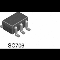
DG2002DL-T1-E3 Vishay, DG2002DL-T1-E3 Datasheet

DG2002DL-T1-E3
Specifications of DG2002DL-T1-E3
Related parts for DG2002DL-T1-E3
DG2002DL-T1-E3 Summary of contents
Page 1
... Battery operated systems • Sample and hold circuits TRUTH TABLE Logic NO (Source ) 1 COM NC (Source ) 2 ORDERING INFORMATION Temp Range - °C DG2002 Vishay Siliconix : 7 Ω DS(on ns OFF : 5 pC INJ OFF Package Part Number DG2002DL-T1 SC70-6 DG2002DL-T1-E3 www.vishay.com Pb-free Available RoHS* COMPLIANT NO OFF ON 1 ...
Page 2
... DG2002 Vishay Siliconix ABSOLUTE MAXIMUM RATINGS Parameter Referenced V+ to GND a IN, COM, NC, NO Continuous Current (Any Terminal) Peak Current (Pulsed duty cycle) Storage Temperature b Power Dissipation (Packages) Notes: a. Signals on NC, NO, or COM or IN exceeding V+ will be clamped by internal diodes. Limit forward diode current to maximum current ratings. ...
Page 3
... NO NC COM 300 Ω 2 Figures 1 and Ω, Figure nF GEN GEN = 50 Ω pF MHz V MHz DG2002 Vishay Siliconix Limits - ° Temp Min Typ Max Unit Full Room 12.2 14.8 Full 13 15.8 Ω Room 5 Room - 500 500 pA nA Full - 4.0 4.0 Room - 500 500 ...
Page 4
... DG2002 Vishay Siliconix SPECIFICATIONS V+ = 5.0 V Parameter Symbol Analog Switch NC, d Analog Signal Range V COM r On-Resistance Flatness ON Flatness I NO(off), I NC(off) Switch Off Leakage Current I COM(off) I Channel-On Leakage Current COM(on) Digital Control V Input High Voltage INH V Input Low Voltage INL C Input Capacitance Input Current ...
Page 5
... on Temperature (°C) Leakage Current vs. Temperature Document Number: 71448 S-72609-Rev. C, 24-Dec- 100 µ 100 100 - 100 - 150 100 DG2002 Vishay Siliconix °C 25 ° ° Analog Voltage ( vs. Analog Voltage and Temperature µ 1 µ 100 100 K Input Switching Frequency (Hz) Supply Current vs. Input Switching Frequency ...
Page 6
... DG2002 Vishay Siliconix TYPICAL CHARACTERISTICS 25 °C, unless otherwise noted Temperature (°C) Switching Time vs. Temperature and Supply Voltage 1.8 1.6 1.4 1.2 1.0 0.8 0.6 0.4 0.2 0 Supply Voltage (V) Switching Threshold vs. Supply Voltage www.vishay.com OFF - OFF - OFF - 90 - 100 100 - LOSS OIRR TALK ...
Page 7
... Figure 1. Switching Time V Logic Input 300 Ω Switch Output Figure 2. Break-Before-Make Interval V V OUT Figure 3. Charge Injection Vishay Siliconix V INH INL Logic "1" = Switch On Logic input waveforms inverted for switches that have the opposite logic sense. INH INL ΔV OUT OUT IN On Off Q = Δ ...
Page 8
... Analyzer 0 V, 2.4 V Vishay Siliconix maintains worldwide manufacturing capability. Products may be manufactured at one of several qualified locations. Reliability data for Silicon Technology and Package Reliability represent a composite of all qualified locations. For related documents such as package/tape drawings, part marking, and reliability data, see http://www.vishay.com/ppg?71448. ...
Page 9
... Vishay product could result in personal injury or death. Customers using or selling Vishay products not expressly indicated for use in such applications their own risk and agree to fully indemnify and hold Vishay and its distributors harmless from and against any and all claims, liabilities, expenses and damages arising or resulting in connection with such use or sale, including attorneys fees, even if such claim alleges that Vishay or its distributor was negligent regarding the design or manufacture of the part ...


