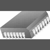
DP8573AV National Semiconductor, DP8573AV Datasheet - Page 12

DP8573AV
Manufacturer Part Number
DP8573AV
Description
Clock IC
Manufacturer
National Semiconductor
Datasheet
1.DP8573AV.pdf
(16 pages)
Specifications of DP8573AV
Date Format
BCD
Clock Format
12 Or 24 Hr
Clock Ic Type
RTC
Digital Ic Case Style
LCC
No. Of Pins
28
Peak Reflow Compatible (260 C)
No
Supply Voltage Max
5.5V
Leaded Process Compatible
No
Mounting Type
Surface Mount
Lead Free Status / RoHS Status
Contains lead / RoHS non-compliant
Available stocks
Company
Part Number
Manufacturer
Quantity
Price
Company:
Part Number:
DP8573AV
Manufacturer:
NSC
Quantity:
5 510
Part Number:
DP8573AV
Manufacturer:
NS/国半
Quantity:
20 000
Company:
Part Number:
DP8573AV/NOPB
Manufacturer:
Renesas
Quantity:
207
Company:
Part Number:
DP8573AV/NOPB
Manufacturer:
Texas Instruments
Quantity:
10 000
Functional Description
D0 –D1 These are the leap year counter bits These bits are
written to set the number of years from the previous leap
year The leap year counter increments on December 31st
and it internally enables the February 29th counter state
This method of setting the leap year allows leap year to
occur whenever the user wishes to thus providing flexibility
in implementing Japanese leap year function
D2 The count mode for the hours counter can be set to
either 24 hour mode or 12 hour mode with AM PM indicator
A one will place the clock in 12 hour mode
D3 This bit is the master Start Stop bit for the clock When
a one is written to this bit the real time counter’s prescaler
and counter chain are enabled When this bit is reset to zero
the contents of the real time counter is stopped When the
RTC is initially powered up this bit will be held at a logic 0
until the oscillator starts functioning correctly after which
this bit may be modified If an oscillator fail event occurs
this bit will be reset to logic 0
D4 This bit controls the operation of the interrupt output in
standby mode If set to a one it allows Alarm Periodic and
Power Fail interrupts to be functional in standby mode Note
that the MFO pin is configured as open drain in standby
mode
If bit D4 is set to a zero then bits D0–D5 of Interrupt Control
Register 0 and bits D6 and D7 of Interrupt Control Register
1 will be reset when the RTC enters the standby mode
They will have to be re-configured when system (V
er is restored
D5 –D7 General purpose RAM bits
OUTPUT MODE REGISTER
D0–D6 General purpose RAM bits
D7 This bit is used to program the signal appearing at the
MFO output as follows
LY1
0
0
1
1
D7
0
1
LY0
0
1
0
1
Power Fail Interrupt
Buffered Crystal Oscillator
MFO Output Signal
Leap Year Current Year
Leap Year Last Year
Leap Year 2 Years Ago
Leap Year 3 Years Ago
Leap Year
(Continued)
Counter
TL F 9981– 16
CC
) pow-
12
INTERRUPT CONTROL REGISTER 0
D0– D5 These bits are used to enable one of the selected
periodic interrupts by writing a one into the appropriate bit
These interrupts are issued at the rollover of the clock For
example the minutes interrupt will be issued whenever the
minutes counter increments In all likelihood the interrupt
will be enabled asynchronously with the real time change
Therefore the very first interrupt will occur in less than the
periodic time chosen but after the first interrupt all subse-
quent interrupts will be spaced correctly These interrupts
are useful when minute second real time reading or task
switching is required When all six bits are written to a 0 this
disables periodic interrupts from the Main Status Register
and the interrupt pin If battery backed mode is selected and
the DP8573A is in standby (V
controlled by D4 of the Real Time Mode Register
D6 and D7 General purpose RAM
INTERRUPT CONTROL REGISTER 1
D0– D5 Each of these bits are enable bits which will enable
a comparison between an individual clock counter and its
associated compare RAM If any bit is a zero then that
clock-RAM comparator is set to the ‘‘always equal’’ state
and the associated TIME COMPARE RAM byte can be used
as general purpose RAM However to ensure that an alarm
interrupt is not generated at bit D3 of the Main Status Regis-
ter all bits must be written to a logic zero
D6 In order to generate an external alarm compare inter-
rupt to the P from bit D3 of the Main Status Register this
bit must be written to a logic 1 If battery backed mode is
selected and the DP8573A is in standby (V
this bit is controlled by D4 of the Real Time Mode Register
D7 The MSB of this register is the enable bit for the Power
Fail Interrupt When this bit is set to a one an interrupt will
be generated to the P when V
mode is selected and the DP8573A is in standby (V
V
Mode Register
CC
) then this bit is controlled by D4 of the Real Time
BB l
BB l
V
CC
V
CC
) then these bits are
If battery backed
BB l
TL F 9981– 17
TL F 9981– 18
V
CC
) then
BB l


