DS34LV86TM National Semiconductor, DS34LV86TM Datasheet

Line Receiver IC

DS34LV86TM

Manufacturer Part Number
DS34LV86TM
Description
Line Receiver IC
Manufacturer
National Semiconductor
Datasheet

Specifications of DS34LV86TM

Driver Case Style
NSOIC
No. Of Pins
16
No. Of Driver/receivers
0/1
Peak Reflow Compatible (260 C)
No
Supply Voltage
3.3V
Current Rating
25A
Supply Voltage Max
3.3V
Leaded Process Compatible
No
Interface Circuit Standard 1
EIA/TIA-422-B/RS-422
Number Of Receivers
4
Number Of Transmitters
Not Required
Number Of Transceivers
Not Required
Data Transmission Topology
Multidrop
Receiver Signal Type
Differential
Transmitter Signal Type
Not Required
Single Supply Voltage (typ)
3.3V
Single Supply Voltage (min)
3V
Single Supply Voltage (max)
3.6V
Dual Supply Voltage (typ)
Not RequiredV
Dual Supply Voltage (min)
Not RequiredV
Dual Supply Voltage (max)
Not RequiredV
Supply Current
15mA
Power Supply Requirement
Single
Operating Temp Range
-40C to 85C
Operating Temperature Classification
Industrial
Mounting
Surface Mount
Pin Count
16
Package Type
SOIC N
Lead Free Status / RoHS Status
Contains lead / RoHS non-compliant
Lead Free Status / RoHS Status
Contains lead / RoHS non-compliant

Available stocks

Company
Part Number
Manufacturer
Quantity
Price
Part Number:
DS34LV86TM
Manufacturer:
national
Quantity:
2 175
Part Number:
DS34LV86TM
Manufacturer:
NS/国半
Quantity:
20 000
Company:
Part Number:
DS34LV86TM
Quantity:
110
Part Number:
DS34LV86TM/NOPB
Manufacturer:
NS
Quantity:
96
Part Number:
DS34LV86TM/NOPB
Manufacturer:
NS
Quantity:
20 000
Part Number:
DS34LV86TMX
Manufacturer:
NS/国半
Quantity:
20 000
Part Number:
DS34LV86TMX
0
Part Number:
DS34LV86TMX/NOPB
0
© 2008 National Semiconductor Corporation
DS34LV86T
3V Enhanced CMOS Quad Differential Line Receiver
General Description
The DS34LV86T is a high speed quad differential CMOS re-
ceiver that meets the requirements of both TIA/EIA-422-B and
ITU-T V.11. The CMOS DS34LV86T features typical low stat-
ic I
power conscious applications. The TRI-STATE
EN, allow the device to be disabled when not in use to mini-
mize power consumption. The dual enable scheme allows for
flexibility in turning receivers on and off.
The receiver output (RO) is guaranteed to be High when the
inputs are left open. The receiver can detect signals as low
as ±200 mV over the common mode range of ±10V. The re-
ceiver outputs (RO) are compatible with TTL and LVCMOS
levels.
Connection Diagram
TRI-STATE
CC
of 9 mA which makes it ideal for battery powered and
®
is a registered trademark of National Semiconductor Corporation.
See NS Package Number M16A
Order Number DS34LV86TM
Dual-In-Line Package
Top View
12644
1264401
®
enables,
Features
Truth Table
L = Logic Low
H = Logic High
X = Irrelevant
Z = TRI-STATE
† = Open, Not Terminated
Low power CMOS design (30 mW typical)
Interoperable with existing 5V RS-422 networks
Industrial temperature range
Meets TIA/EIA-422-B (RS-422) and ITU-T V.11
recommendation
3.3V Operation
±7V common mode range @ V
±10V common mode range @ V
Receiver OPEN input failsafe feature
Guaranteed AC parameter:
Pin compatible with DS34C86T
32 MHz Toggle Frequency
>6.5k ESD Tolerance (HBM)
Available in SOIC packaging
Maximum Receiver Skew: 4 ns
Transition time: 10 ns
Enable
EN
H
H
H
L
V
V
ID
ID
RI+–RI−
Inputs
Open†
X
+0.2V
−0.2V
ID
ID
= 3V
= 0.2V
September 11, 2008
www.national.com
Output
RO
H
H
Z
L

Related parts for DS34LV86TM

DS34LV86TM Summary of contents

Page 1

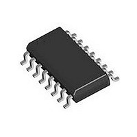
... The re- ceiver outputs (RO) are compatible with TTL and LVCMOS levels. Connection Diagram Dual-In-Line Package Top View Order Number DS34LV86TM See NS Package Number M16A TRI-STATE ® registered trademark of National Semiconductor Corporation. © 2008 National Semiconductor Corporation Features ■ ...

Page 2

... Absolute Maximum Ratings If Military/Aerospace specified devices are required, please contact the National Semiconductor Sales Office/ Distributors for availability and specifications. Supply Voltage ( Enable Input Voltage (EN) Receiver Input Voltage (V : RI+, RI−) ID Receiver Input Voltage (V : RI+, RI−) CM Receiver Output Voltage (RO) Receiver Output Current (RO) Maximum Package Power Dissipation @ +25° ...

Page 3

Switching Characteristics Over Supply Voltage and Operating Temperature ranges, unless otherwise specified. Symbol Parameter t Propagation Delay High to Low PHL t Propagation DeIay Low to High PLH t Rise Time (20 Fall Time (80% to ...

Page 4

FIGURE 2. Receiver Propagation Delay and Transition Time Waveform (Notes 9, 10) Note 9: Generator waveform for all tests unless otherwise specified MHz, Duty Cycle = 50%, Z Note 10: C includes probe and jig capacitance. L ...

Page 5

Typical Application Information General application guidelines and hints for differential drivers receivers may be found in the following application notes: AN-214, AN-457, AN-805, AN-847, AN-903, AN-912, AN-916 Power Decoupling Recommendations: Bypass caps must be used on power pins. High frequency ...

Page 6

FIGURE 7. Typical Receiver Input Circuit FIGURE 8. Typical I vs Frequency CC 6 1264409 1264410 ...

Page 7

FIGURE (Power On, Power Off FIGURE 10 1264411 1264412 www.national.com ...

Page 8

FIGURE 11 1264413 ...

Page 9

... Physical Dimensions inches (millimeters) unless otherwise noted Dual-In-Line Package Order Number DS34LV86TM NS Package Number M16A 9 www.national.com ...

Page 10

... For more National Semiconductor product information and proven design tools, visit the following Web sites at: Products Amplifiers www.national.com/amplifiers Audio www.national.com/audio Clock Conditioners www.national.com/timing Data Converters www.national.com/adc Displays www.national.com/displays Ethernet www.national.com/ethernet Interface www.national.com/interface LVDS www.national.com/lvds Power Management www.national.com/power Switching Regulators www.national.com/switchers LDOs www ...

Related keywords