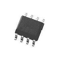
DS90C402M National Semiconductor, DS90C402M Datasheet - Page 4

DS90C402M
Manufacturer Part Number
DS90C402M
Description
LVDS Line Receiver IC
Manufacturer
National Semiconductor
Specifications of DS90C402M
No. Of Drivers
2
Driver Case Style
NSOIC
No. Of Pins
8
Mounting Type
Surface Mount
No. Of Driver/receivers
2/0
Peak Reflow Compatible (260 C)
No
Supply Voltage
5V
Supply Voltage Max
5V
Lead Free Status / RoHS Status
Contains lead / RoHS non-compliant
Available stocks
Company
Part Number
Manufacturer
Quantity
Price
Company:
Part Number:
DS90C402M
Manufacturer:
ns
Quantity:
2 602
Part Number:
DS90C402M
Manufacturer:
NS/国半
Quantity:
20 000
Company:
Part Number:
DS90C402M/NOPB
Manufacturer:
NSC
Quantity:
650
Part Number:
DS90C402MX
Manufacturer:
NS/国半
Quantity:
20 000
Company:
Part Number:
DS90C402MX/NOPB
Manufacturer:
ACTEL
Quantity:
210
Part Number:
DS90C402MX/NOPB
Manufacturer:
TI/德州仪器
Quantity:
20 000
www.national.com
Applications Information
1. Open Input Pins. The DS90C402 is a dual receiver
2. Terminated Input. If the driver is disconnected (cable
3. Shorted Inputs. If a fault condition occurs that shorts
Note 1: “Absolute Maximum Ratings” are those values beyond which the safety of the device cannot be guaranteed. They are not meant to imply that the devices
should be operated at these limits. The table of “Electrical Characteristics” specifies conditions of device operation.
Note 2: Current into device pins is defined as positive. Current out of device pins is defined as negative. All voltages are referenced to ground unless otherwise
specified.
Note 3: All typicals are given for: V
Note 4: Generator waveform for all tests unless otherwise specified: f = 1 MHz, Z
Note 5: Channel-to-Channel Skew is defined as the difference between the propagation delay of one channel and that of the others on the same chip with an event
on the inputs.
Note 6: Chip to Chip Skew is defined as the difference between the minimum and maximum specified differential propagation delays.
Note 7: ESD Rating:
Note 8: Output short circuit current (I
exceed maximum junction temperature specification.
Note 9: C
HBM (1.5 kΩ, 100 pF) ≥ 3,500V
EIAJ (0Ω, 200 pF) ≥ 250V
device, and if an application requires only one receiver,
the unused channel(s) inputs should be left OPEN. Do
not tie unused receiver inputs to ground or any other
voltages. The input is biased by internal high value pull
up and pull down resistors to set the output to a HIGH
state. This internal circuitry will guarantee a HIGH,
stable output state for open inputs.
unplugged), or if the driver is in a power-off condition,
the receiver output will again be in a HIGH state, even
with the end of cable 100Ω termination resistor across
the input pins. The unplugged cable can become a
floating antenna which can pick up noise. If the cable
picks up more than 10mV of differential noise, the re-
ceiver may see the noise as a valid signal and switch. To
insure that any noise is seen as common-mode and not
differential, a balanced interconnect should be used.
Twisted pair cable will offer better balance than flat
ribbon cable
the receiver inputs together, thus resulting in a 0V differ-
L
includes probe and jig capacitance.
CC
OS
= +5.0V, T
) is specified as magnitude only, minus sign indicates direction only. Only one output should be shorted at a time, do not
H = Logic High Level
L = Logic Low level
X = Indeterminant State
A
= +25˚C.
(Continued)
100 mV
R
>
<
RECEIVE MODE
IN+
>
+100 mV
−100 mV
&
− R
>
IN−
−100 mV
4
O
= 50Ω, t
Pin Descriptions
Ordering Information
Pin No.
−40˚C to +85˚C
2, 6
3, 7
4, 8
Temperature
ential input voltage, the receiver output will remain in a
HIGH state. Shorted input fail-safe is not supported
across the common-mode range of the device (GND to
2.4V). It is only supported with inputs shorted and no
external common-mode voltage applied.
5
1
Operating
r
and t
f
Name
(0%–100%) ≤ 1 ns for R
R
GND
R
R
V
R
OUT
IN
CC
IN
OUT
H
X
L
+
-
Receiver output pin
Positive receiver input pin
Negative receiver input pin
Ground pin
Positive power supply pin,
+5V
Package Type/
SOP/M08A
±
Number
10%
IN
.
Description
Order Number
DS90C402M


