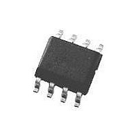
DS90LV027ATM National Semiconductor, DS90LV027ATM Datasheet - Page 3

DS90LV027ATM
Manufacturer Part Number
DS90LV027ATM
Description
Driver IC
Manufacturer
National Semiconductor
Specifications of DS90LV027ATM
Driver Case Style
NSOIC
No. Of Pins
8
No. Of Driver/receivers
2/0
Peak Reflow Compatible (260 C)
No
Supply Voltage
3.3V
Supply Voltage Max
3.3V
Leaded Process Compatible
No
Mounting Type
Surface Mount
Lead Free Status / RoHS Status
Contains lead / RoHS non-compliant
Available stocks
Company
Part Number
Manufacturer
Quantity
Price
Company:
Part Number:
DS90LV027ATM
Manufacturer:
nstion
Quantity:
427
Part Number:
DS90LV027ATM
Manufacturer:
NS/国半
Quantity:
20 000
Part Number:
DS90LV027ATMX
Manufacturer:
NS/国半
Quantity:
20 000
Company:
Part Number:
DS90LV027ATMX/NOPB
Manufacturer:
NS
Quantity:
8 913
Switching Characteristics
Note 6: Generator waveform for all tests unless otherwise specified: f = 1 MHz, Z
Note 7: The DS90LV027A is a current mode device and only function with datasheet specification when a resistive load is applied to the drivers outputs.
Note 8: t
the same channel.
Note 9: t
Note 10: t
specification applies to devices at the same V
Note 11: t
operating temperature and voltage ranges, and across process distribution. t
Note 12: f
switching.
Parameter Measurement Information
SKD1
SKD2
SKD4
SKD3
MAX
, |t
is the Differential Channel to Channel Skew of any event on the same device.
, part to part skew, is the differential channel to channel skew of any event between devices. This specification applies to devices over recommended
generator input conditions: t
, Differential Part to Part Skew, is defined as the difference between the minimum and maximum specified differential propagation delays. This
PHLD
− t
PLHD
FIGURE 2. Differential Driver Propagation Delay and Transition Time Test Circuit
FIGURE 3. Differential Driver Propagation Delay and Transition Time Waveforms
|, is the magnitude difference in differential propagation delay time between the positive going edge and the negative going edge of
r
= t
CC
f
<
and within 5˚C of each other within the operating temperature range.
1 ns (0% to 100%), 50% duty cycle, 0V to 3V. Output criteria: duty cycle = 45%/55%, V
FIGURE 1. Differential Driver DC Test Circuit
(Continued)
SKD4
3
is defined as |Max − Min| differential propagation delay.
O
= 50Ω, t
r
≤ 1 ns, t
f
10011405
≤ 1 ns (10%-90%).
10011406
10011404
OD
>
250mV, all channels
www.national.com


