LM193H National Semiconductor, LM193H Datasheet - Page 4
LM193H
Manufacturer Part Number
LM193H
Description
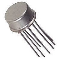
IC, PRECISION COMP, DUAL, 300NS, TO-99-8
Manufacturer
National Semiconductor
Datasheet
1.LM193H.pdf
(15 pages)
Specifications of LM193H
Comparator Type
Precision
No. Of Comparators
2
Response Time
300ns
Supply Current
1mA
Supply Voltage Range
± 1V To ± 18V
Amplifier Case Style
TO-99
No. Of Pins
8
Lead Free Status / RoHS Status
Contains lead / RoHS non-compliant
Available stocks
Company
Part Number
Manufacturer
Quantity
Price


www.national.com
Supply Current
Voltage Gain
Large Signal Response
Time
Response Time
Output Sink Current
Saturation Voltage
Output Leakage Current
Input Offset Voltage
Input Offset Current
Input Bias Current
Input Common Mode
Voltage Range
Saturation Voltage
Output Leakage Current
Differential Input Voltage
Electrical Characteristics
(V
Electrical Characteristics
Input Offset Voltage
Input Offset Current
Input Bias Current
Input Common Mode
Voltage Range
Saturation Voltage
Output Leakage Current
Differential Input Voltage
Electrical Characteristics
(V+ = 5V) (Note 4)
Note 1: For operating at high temperatures, the LM393 and LM2903 must be derated based on a 125˚C maximum junction temperature and a thermal resistance
of 170˚C/W which applies for the device soldered in a printed circuit board, operating in a still air ambient. The LM193/LM193A/LM293 must be derated based on
a 150˚C maximum junction temperature. The low bias dissipation and the “ON-OFF” characteristic of the outputs keeps the chip dissipation very small (P
provided the output transistors are allowed to saturate.
Note 2: Short circuits from the output to V
current is approximately 20 mA independent of the magnitude of V
Note 3: This input current will only exist when the voltage at any of the input leads is driven negative. It is due to the collector-base junction of the input PNP
transistors becoming forward biased and thereby acting as input diode clamps. In addition to this diode action, there is also lateral NPN parasitic transistor action
(V+ = 5V) (Note 4)
+
=5V, T
Parameter
Parameter
Parameter
A
= 25˚C, unless otherwise stated)
R
R
V
V
V
V
V
V
V
(Note 9)
I
I
Linear Range, V
(Note 5)
V
V
I
V
Keep All V
Used), (Note 8)
IN(+)
IN
SINK
O
IN
RL
RL
IN
IN
IN
L
L
+
IN
IN
≥15 kΩ, V
=
(+) or I
(−)=1V, V
(−)=1V, V
(−)=0, V
=30V (Note 6)
=TTL Logic Swing, V
= 1V to 11V
=5V, R
=5V, R
(−)=1V, V
(−)=0, V
∞
−I
≤4 mA
IN(−)
+
can cause excessive heating and eventual destruction. When considering short circuits to ground, the maximum output
IN
(Note 9)
I
I
V
V
V
V
Keep All V
L
L
Conditions
IN(+)
IN
, V
IN
(−) with Output in
IN
=5.1 kΩ
=5.1 kΩ (Note 7)
CM
+
IN
IN
IN(+)
+
(+) or I
’s≥0V (or V
V
V
IN
IN
=30V (Note 6)
Conditions
(+)=1V, V
(−)=1V, V
(−)=0, V
IN
=15V
CM
+
+
(+)=0, V
(+)=0, I
=0V (Note 5)
−I
(+)=0,
=5V
=36V
=1V, V
=0V
IN(−)
CM
(Continued)
IN
=0V
, V
IN
(−) with Output in Linear Range,
IN(+)
SINK
’s≥0V (or V
O
O
O
IN
CM
−
REF
≤1.5V
=5V
=30V
, if
(+)=0, I
=1V, V
≤4 mA
=0V
+
Conditions
=1.4V
.
SINK
O
−
=30V
Min Typ
, if Used), (Note 8)
0
≤4 mA
4
Min Typ
LM193
6.0
50 200
LM193
300
250
0.4
1.3
0.1
V
16
1
Max
+
100
300
700
1.0
36
−2.0
9
Max
400
2.5
1
Min Typ
LM293, LM393
0
Min Typ
6.0
50 200
LM293, LM393
Min
0
300
250
0.4
1.3
0.1
16
1
V
Max
+
150
400
700
1.0
36
−2.0
9
Max
400
LM193A
2.5
1
Typ
Min Typ
0
Min Typ
6.0
25 100
LM2903
200
400
50
V
9
LM2903
+
300
250
0.4
1.5
0.1
Max
16
100
300
700
−2.0
4.0
1.0
1
36
V
Max
+
200
500
700
1.0
15
36
−2.0
Max
400
1.0
2.5
D
≤100 mW),
Units
mV
mV
nA
nA
µA
Units
V
V
Units
V/mV
mV
mV
nA
nA
µA
mA
mA
mA
mV
nA
ns
µs
V
V
Related parts for LM193H
Image
Part Number
Description
Manufacturer
Datasheet
Request
R

Part Number:
Description:
LM193/LM293/LM393/LM2903 Low Power Low Offset Voltage Dual Comparators; ; Container: Tray
Manufacturer:
National Semiconductor
Part Number:
Description:
Low Power Low Offset Voltage Dual Comparator
Manufacturer:
National Semiconductor
Part Number:
Description:
LM193/LM293/LM393/LM2903 Low Power Low Offset Voltage Dual Comparators; ; Container: Tray
Manufacturer:
National Semiconductor
Part Number:
Description:
National Semiconductor [8-Bit D/A Converter]
Manufacturer:
National Semiconductor
Datasheet:
Part Number:
Description:
National Semiconductor [Media Coprocessor]
Manufacturer:
National Semiconductor
Datasheet:
Part Number:
Description:
Digitally Controlled Tone and Volume Circuit with Stereo Audio Power Amplifier, Microphone Preamp Stage and National 3D Sound
Manufacturer:
National Semiconductor
Datasheet:
Part Number:
Description:
Digitally Controlled Tone and Volume Circuit with Stereo Audio Power Amplifier, Microphone Preamp Stage and National 3D Sound
Manufacturer:
National Semiconductor
Datasheet:
Part Number:
Description:
AC97 Rev 2 Codec with Sample Rate Conversion and National 3D Sound
Manufacturer:
National Semiconductor
Part Number:
Description:
Manufacturer:
National Semiconductor
Datasheet:
Part Number:
Description:
Manufacturer:
National Semiconductor
Datasheet:
Part Number:
Description:
General Purpose, Low Voltage, Low Power, Rail-to-Rail Output Operational Amplifiers
Manufacturer:
National Semiconductor
Datasheet:
Part Number:
Description:
8-bit 20 MSPS flash A/D converter.
Manufacturer:
National Semiconductor
Datasheet:
Part Number:
Description:
Low Noise Quad Operational Amplifier
Manufacturer:
National Semiconductor
Datasheet:
Part Number:
Description:
Quad Differential Line Receivers
Manufacturer:
National Semiconductor
Datasheet: