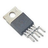
LM2592HVT-ADJ National Semiconductor, LM2592HVT-ADJ Datasheet - Page 3

LM2592HVT-ADJ
Manufacturer Part Number
LM2592HVT-ADJ
Description
Voltage Regulator IC
Manufacturer
National Semiconductor
Specifications of LM2592HVT-ADJ
Input Voltage
60V
Output Current
2A
Output Voltage
57V
No. Of Pins
5
Termination Type
Through Hole
Mounting Type
Through Hole
Voltage Regulator Type
Buck Switching
Output Current Max
2A
Lead Free Status / RoHS Status
Contains lead / RoHS non-compliant
Available stocks
Company
Part Number
Manufacturer
Quantity
Price
Company:
Part Number:
LM2592HVT-ADJ
Manufacturer:
NS
Quantity:
500
DEVICE PARAMETERS
I
f
V
DC
I
I
I
I
ON/OFF CONTROL Test Circuit Figure 1
V
V
I
I
b
O
CLIM
L
Q
STBY
H
L
Symbol
JC
JA
JA
JA
JA
SAT
IH
IL
All Output Voltage Versions
Electrical Characteristics
Specifications with standard type face are for T
ture Range. Unless otherwise specified, V
Note 1: Absolute Maximum Ratings indicate limits beyond which damage to the device may occur. Operating Ratings indicate conditions for which the device is
intended to be functional, but do not guarantee specific performance limits. For guaranteed specifications and test conditions, see the Electrical Characteristics.
Note 2: The human body model is a 100 pF capacitor discharged through a 1.5k resistor into each pin.
Note 3: Typical numbers are at 25˚C and represent the most likely norm.
Note 4: All limits guaranteed at room temperature (standard type face) and at temperature extremes (bold type face). All room temperature limits are 100%
production tested. All limits at temperature extremes are guaranteed via correlation using standard Statistical Quality Control (SQC) methods. All limits are used
to calculate Average Outgoing Quality Level (AOQL).
Note 5: External components such as the catch diode, inductor, input and output capacitors can affect switching regulator system performance. When the
LM2592HV is used as shown in the Figure 1 test circuit, system performance will be as shown in system parameters section of Electrical Characteristics.
Note 6: The switching frequency is reduced when the second stage current limit is activated. The amount of reduction is determined by the severity of current
overload.
Note 7: No diode, inductor or capacitor connected to output pin.
Note 8: Feedback pin removed from output and connected to 0V to force the output transistor switch ON.
Note 9: Feedback pin removed from output and connected to 12V for the 3.3V, 5V, and the ADJ. version to force the output transistor switch OFF.
Note 10: V
IN
Feedback Bias Current
Oscillator Frequency
Saturation Voltage
Max Duty Cycle (ON)
Min Duty Cycle (OFF)
Switch current Limit
Output Leakage Current
Operating Quiescent
Current
Standby Quiescent
Current
Thermal Resistance
ON /OFF Pin Logic Input
Threshold Voltage
ON /OFF Pin Input Current
= 60V.
Parameter
IN
Adjustable Version Only, V
(Note 6)
I
(Note 8)
(Note 9)
Peak Current, (Note 7) (Note 8)
(Note 7) (Note 9) (Note 10)
SD /SS Pin Open (Note 9)
SD /SS pin = 0V
TO220 or TO263 Package, Junction to Case
TO220 Package, Juncton to Ambient (Note 11)
TO263 Package, Juncton to Ambient (Note 12)
TO263 Package, Juncton to Ambient (Note 13)
TO263 Package, Juncton to Ambient (Note 14)
Low (Regulator ON)
High (Regulator OFF)
V
V
OUT
LOGIC
LOGIC
= 12V for the 3.3V, 5V, and Adjustable version. I
J
= 2A (Note 7) (Note 8)
= 25˚C, and those with boldface type apply over full Operating Tempera-
= 2.5V (Regulator OFF)
= 0.5V (Regulator ON)
Conditions
3
(Note 10)
FB
= 1.3V
Output = 0V
Output = −1V
LOAD
(Note 3)
1.10
0.02
Typ
150
100
LM2592HV-XX
3.0
1.3
10
90
50
50
30
20
0
5
5
2
5
= 500 mA
(Note 4)
127/110
173/173
200/250
50/100
1.3/1.4
2.4/2.3
3.7/4.0
Limit
0.6
2.0
50
30
10
15
5
www.national.com
kHz(max)
nA (max)
kHz(min)
mA(max)
mA(max)
µA(max)
µA(max)
µA(max)
µA(max)
(Limits)
V(max)
A(max)
V(max)
A(min)
V(min)
Units
˚C/W
˚C/W
˚C/W
˚C/W
˚C/W
kHz
mA
mA
nA
µA
µA
µA
%
V
A
V


