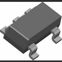
LM4120IM5-2.5 National Semiconductor, LM4120IM5-2.5 Datasheet - Page 9

LM4120IM5-2.5
Manufacturer Part Number
LM4120IM5-2.5
Description
Voltage Reference
Manufacturer
National Semiconductor
Type
Precision Micropower Low Dropout Voltage Referencer
Datasheets
1.LM4120IM5-2.5.pdf
(12 pages)
2.LM4120IM5-2.5.pdf
(11 pages)
3.LM4120IM5-2.5.pdf
(11 pages)
Specifications of LM4120IM5-2.5
Peak Reflow Compatible (260 C)
No
Leaded Process Compatible
No
Mounting Type
Surface Mount
Voltage Regulator Type
LDO Linear
Package / Case
SOT-23
Lead Free Status / RoHS Status
Contains lead / RoHS non-compliant
Available stocks
Company
Part Number
Manufacturer
Quantity
Price
Company:
Part Number:
LM4120IM5-2.5
Manufacturer:
NS
Quantity:
5 087
Part Number:
LM4120IM5-2.5
Manufacturer:
NS/国半
Quantity:
20 000
LM4120 Typical Operating Characteristics
I
Pin Functions
Output (Pin 5): Reference Output.
Input (Pin 4):Positive Supply.
Ground (Pin 2):Negative Supply or Ground Connection.
Enable (Pin 3):Pulled to input for normal operation. Forcing
this pin to ground will turn-off the output.
REF (Pin 1):REF Pin. This pin should be left unconnected.
Application Hints
The standard application circuit for the LM4120 is shown in
Figure 1. It is designed to be stable with ceramic output
capacitors in the range of 0.022µF to 0.047µF. Note that
0.022µF is the minimum required output capacitor. These
capacitors typically have an ESR of about 0.1 to 0.5Ω.
Smaller ESR can be tolerated, however larger ESR can not.
The output capacitor can be increased to improve load tran-
sient response, up to about 1µF. However, values above
0.047µF must be tantalum. With tantalum capacitors, in the
1µF range, a small capacitor between the output and the
reference pin is required. This capacitor will typically be in
the 50pF range. Care must be taken when using output
capacitors of 1µF or larger. These application must be thor-
oughly tested over temperature, line and load.
An input capacitor is typically not required. However, a 0.1µF
ceramic can be used to help prevent line transients from
entering the LM4120. Larger input capacitors should be
tantalum or aluminium.
The reference pin is sensitive to noise, and capacitive load-
ing. Therefore, the PCB layout should isolate this pin as
much as possible.
The enable pin is an analog input with very little hysteresis.
About 6µA into this pin is required to turn the part on, and it
LOAD
= 0, C
OUT
= 0.022µF, T
Thermal Hysteresis
A
= 25˚C and V
10104731
EN
= V
IN
. (Continued)
9
must be taken close to GND to turn the part off (see spec.
table for thresholds). There is a minimum slew rate on this
pin of about 0.003V/µS to prevent glitches on the output. All
of these conditions can easily be met with ordinary CMOS or
TTL logic. If the shutdown feature is not required, then this
pin can safely be connected directly to the input supply.
Floating this pin is not recommended.
INPUT CAPACITOR
Noise on the power-supply input can effect the output noise,
but can be reduced by using an optional bypass capacitor
between the input pin and the ground.
PRINTED CIRCUIT BOARD LAYOUT CONSIDERATION
The mechanical stress due to PC board mounting can cause
the output voltage to shift from its initial value. References in
SOT packages are generally less prone to assembly stress
than devices in Small Outline (SOIC) package.
To reduce the stress-related output voltage shifts, mount the
reference on the low flex areas of the PC board such as near
to the edge or the corner of the PC board.
Unless otherwise specified, V
Enable Pin Current
FIGURE 1.
IN
10104732
= 3.3V, V
10104716
OUT
www.national.com
= 2.5V,


