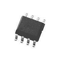
LM6181IM-8 National Semiconductor, LM6181IM-8 Datasheet - Page 18

LM6181IM-8
Manufacturer Part Number
LM6181IM-8
Description
Operational Amplifier (Op-Amp) IC
Manufacturer
National Semiconductor
Specifications of LM6181IM-8
No. Of Amplifiers
1
Bandwidth
100MHz
No. Of Pins
8
Peak Reflow Compatible (260 C)
No
Leaded Process Compatible
No
Mounting Type
Surface Mount
Package / Case
8-NSOIC
Number Of Channels
1
Common Mode Rejection Ratio (min)
50 dB
Input Offset Voltage
3 mV at +/- 5 V
Operating Supply Voltage
9 V, 12 V, 15 V, 18 V, 24 V, 28 V
Supply Current
8.5 mA at +/- 5 V
Maximum Operating Temperature
+ 85 C
Maximum Dual Supply Voltage
+/- 16 V
Minimum Operating Temperature
- 40 C
Lead Free Status / RoHS Status
Contains lead / RoHS non-compliant
Available stocks
Company
Part Number
Manufacturer
Quantity
Price
Company:
Part Number:
LM6181IM-8
Manufacturer:
NS
Quantity:
345
Part Number:
LM6181IM-8
Manufacturer:
NS/国半
Quantity:
20 000
Company:
Part Number:
LM6181IM-8/NOPB
Manufacturer:
TI
Quantity:
25
www.national.com
Typical Applications
CAPACITIVE FEEDBACK
For voltage feedback amplifiers it is quite common to place a
small lead compensation capacitor in parallel with feedback
resistance, R
plifier’s peaking in the frequency domain which equivalently
tames the transient response. To limit the bandwidth of cur-
rent feedback amplifiers, do not use a capacitor across R
The dynamic impedance of capacitors in the feedback loop
reduces the amplifier’s stability. Instead, reduced peaking in
the frequency response, and bandwidth limiting can be ac-
complished by adding an RC circuit, as illustrated in Figure
7b .
and R
and Improve Pulse Response Characteristics.
Provides Higher Fidelity Pulse Response. R
S
FIGURE 6. Resistive Isolation of C
Could Be Increased to Maintain A
f
. This compensation serves to reduce the am-
6b
6a
(Continued)
L
DS011328-20
V
= −1
DS011328-21
f
f
.
18
Typical Performance
Characteristics
OVERDRIVE RECOVERY
When the output or input voltage range of a high speed am-
plifier is exceeded, the amplifier must recover from an over-
drive condition. The typical recovery times for open-loop,
closed-loop, and input common-mode voltage range over-
drive conditions are illustrated in Figures 9, 11, 11, 12 re-
spectively.
The open-loop circuit of Figure 8 generates an overdrive re-
sponse by allowing the
put range of the amplifier. Typical positive and negative over-
drive recovery times shown in Figure 9 are 5 ns and 25 ns,
respectively.
Peaking in the Resulting Pulse Response
Bandwidth to 50 MHz, Eliminating
FIGURE 7. RC Limits Amplifier
±
0.5V input to exceed the linear in-
7a
7b
DS011328-22
DS011328-23


