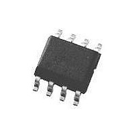
LMC6482IM National Semiconductor, LMC6482IM Datasheet - Page 15

LMC6482IM
Manufacturer Part Number
LMC6482IM
Description
Operational Amplifier (Op-Amp) IC
Manufacturer
National Semiconductor
Datasheet
1.LMC6482IM.pdf
(25 pages)
Specifications of LMC6482IM
No. Of Amplifiers
2
Slew Rate
1.3V/µs
No. Of Pins
8
Peak Reflow Compatible (260 C)
No
Leaded Process Compatible
No
Amplifier Type
Operational
Mounting Type
Surface Mount
Lead Free Status / RoHS Status
Contains lead / RoHS non-compliant
Available stocks
Company
Part Number
Manufacturer
Quantity
Price
Company:
Part Number:
LMC6482IM
Manufacturer:
ns
Quantity:
5 575
Part Number:
LMC6482IM
Manufacturer:
NS/国半
Quantity:
20 000
Company:
Part Number:
LMC6482IM/NOPB
Manufacturer:
TI
Quantity:
3 000
Part Number:
LMC6482IM/NOPB
Manufacturer:
NS/国半
Quantity:
20 000
Company:
Part Number:
LMC6482IMM
Manufacturer:
NS75
Quantity:
984
Part Number:
LMC6482IMM
Manufacturer:
NS/国半
Quantity:
20 000
Company:
Part Number:
LMC6482IMM/NOPB
Manufacturer:
National Semiconductor
Quantity:
25 066
Part Number:
LMC6482IMM/NOPB
Manufacturer:
TI/德州仪器
Quantity:
20 000
Company:
Part Number:
LMC6482IMMX
Manufacturer:
TI
Quantity:
168
Part Number:
LMC6482IMMX
Manufacturer:
NS/国半
Quantity:
20 000
Application Information
Improved frequency response is achieved by indirectly driv-
ing capacitive loads, as shown in Figure 6.
R1 and C1 serve to counteract the loss of phase margin by
feeding forward the high frequency component of the output
signal back to the amplifiers inverting input, thereby preserv-
ing phase margin in the overall feedback loop. The values of
R1 and C1 are experimentally determined for the desired
pulse response. The resulting pulse response can be seen in
Figure 7.
Compensated to Handle a 330pF Capacitive Load
FIGURE 6. LMC6482 Noninverting Amplifier,
the LMC6482 Circuit in Figure 4
FIGURE 5. Pulse Response of
FIGURE 4. Resistive Isolation
of a 330pF Capacitive Load
01171317
(Continued)
01171315
01171318
15
5.0 COMPENSATING FOR INPUT CAPACITANCE
It is quite common to use large values of feedback resis-
tance with amplifiers that have ultra-low input current, like
the LMC6482. Large feedback resistors can react with small
values of input capacitance due to transducers, photo-
diodes, and circuits board parasitics to reduce phase mar-
gins.
The effect of input capacitance can be compensated for by
adding a feedback capacitor. The feedback capacitor (as in
Figure 8), C
which typically provides significant overcompensation.
Printed circuit board stray capacitance may be larger or
smaller than that of a bread-board, so the actual optimum
value for C
checked on the actual circuit. (Refer to the LMC660 quad
CMOS amplifier data sheet for a more detailed discussion.)
FIGURE 8. Canceling the Effect of Input Capacitance
f
f
, is first estimated by:
may be different. The values of C
FIGURE 7. Pulse Response of
LMC6482 Circuit in Figure 6
R
1
C
IN
or
≤ R
2
C
f
f
www.national.com
should be
01171319
01171316


