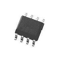
LMH6715MA National Semiconductor, LMH6715MA Datasheet - Page 9

LMH6715MA
Manufacturer Part Number
LMH6715MA
Description
Operational Amplifier (Op-Amp) IC
Manufacturer
National Semiconductor
Datasheet
1.LMH6715MA.pdf
(12 pages)
Specifications of LMH6715MA
Bandwidth
480MHz
Slew Rate
1300V/µs
No. Of Pins
8
Peak Reflow Compatible (260 C)
No
Input Offset Voltage Max
8mV
Leaded Process Compatible
No
Mounting Type
Surface Mount
Package / Case
8-SOIC
Number Of Channels
2
Voltage Gain Db
60 dB
Common Mode Rejection Ratio (min)
50 dB
Input Offset Voltage
6 mV at +/- 5 V
Supply Current
15.2 mA at +/- 5 V
Maximum Operating Temperature
+ 85 C
Maximum Dual Supply Voltage
+/- 6 V
Minimum Operating Temperature
- 40 C
Lead Free Status / RoHS Status
Contains lead / RoHS non-compliant
Available stocks
Company
Part Number
Manufacturer
Quantity
Price
Part Number:
LMH6715MA
Manufacturer:
NS/国半
Quantity:
20 000
Part Number:
LMH6715MAX
Manufacturer:
NS/国半
Quantity:
20 000
Application Introduction
Both plots show the value of R
value (dashed line) at high gains. Reducing the feedback
resistor below this value will result in instability and possibly
oscillation. The recommended value of R
solid line, which begins to increase at higher gains. The
reason that a higher R
need to keep R
impedance of the input buffer. For the LMH6715 the output
resistance of the input buffer is approximately 160Ω and 50Ω
is a practical lower limit for R
the LMH6715 begins to operate in a gain bandwidth limited
fashion for gains of
When using the LMH6715 as a replacement for the CLC412,
identical bandwidth can be obtained by using an appropriate
value of R
that an R
very close to that of the CLC412. At other gains a similar
increase in R
CIRCUIT LAYOUT
With all high frequency devices, board layouts with stray
capacitances have a strong influence over AC performance.
The LMH6715 is no exception and its input and output pins
are particularly sensitive to the coupling of parasitic capaci-
F
F
. The chart “Frequency Response vs. R
of approximately 700Ω will provide bandwidth
F
can be used to match the new and old parts.
G
R
F
from decreasing too far below the output
R
vs. Non-Inverting Gain
±
F
5V/V or greater.
vs. Inverting Gain
F
is required at higher gains is the
G
. Due to the limitations on R
F
approaching a minimum
F
is depicted by the
(Continued)
20042921
20042922
F
” shows
G
9
tances (to AC ground) arising from traces or pads placed too
closely (
due to the frequency response peaking caused by these
parasitics, a small adjustment of the feedback resistor value
will serve to compensate the frequency response. Also, it is
very important to keep the parasitic capacitance across the
feedback resistor to an absolute minimum.
The performance plots in the data sheet can be reproduced
using the evaluation boards available from National. The
CLC730036 board uses all SMT parts for the evaluation of
the LMH6715. The board can serve as an example layout for
the final production printed circuit board.
Care must also be taken with the LMH6715’s layout in order
to achieve the best circuit performance, particularly channel-
to-channel isolation. The decoupling capacitors (both tanta-
lum and ceramic) must be chosen with good high frequency
characteristics to decouple the power supplies and the
physical placement of the LMH6715’s external components
is critical. Grouping each amplifier’s external components
with their own ground connection and separating them from
the external components of the opposing channel with the
maximum possible distance is recommended. The input
(R
also recommended that the ceramic decoupling capacitor
(0.1µF chip or radial-leaded with low ESR) should be placed
as closely to the power pins as possible.
POWER DISSIPATION
Follow these steps to determine the Maximum power dissi-
pation for the LMH6715:
1. Calculate the quiescent (no-load) power: P
- V
2. Calculate the RMS power at the output stage: P
-V
current across the external load.
3. Calculate the total RMS power: Pt = P
The maximum power that the LMH6715, package can dissi-
pate at a given temperature can be derived with the following
equation:
Pmax = (150
ture (˚C) and θ
ambient, for a given package (˚C/W). For the SOIC package
θ
MATCHING PERFORMANCE
With proper board layout, the AC performance match be-
tween the two LMH6715’s amplifiers can be tightly controlled
as shown in Typical Performance plot labeled “Small-Signal
Channel Matching”.
The measurements were performed with SMT components
using a feedback resistor of 300Ω at a gain of +2V/V.
The LMH6715’s amplifiers, built on the same die, provide the
advantage of having tightly matched DC characteristics.
SLEW RATE AND SETTLING TIME
One of the advantages of current-feedback topology is an
inherently high slew rate which produces a wider full power
bandwidth. The LMH6715 has a typical slew rate of 1300V/
µs. The required slew rate for a design can be calculated by
the following equation: SR = 2πfV
Careful attention to parasitic capacitances is critical to
achieving the best settling time performance. The LMH6715
JA
IN
LOAD
EE
is 145˚C/W.
) and gain setting resistors (R
)
)(I
<
LOAD
0.1”) to power or ground planes. In some cases,
o
), where V
- Tamb)/ θ
JA
= Thermal resistance, from junction to
JA
LOAD
, where Tamb = Ambient tempera-
and I
F
pk
) are the most critical. It is
LOAD
.
are the voltage and
AMP
AMP
+ P
www.national.com
= I
O
O
CC
= (V
(V
CC
CC


