MCP73863-I/ML Microchip Technology, MCP73863-I/ML Datasheet - Page 18
MCP73863-I/ML
Manufacturer Part Number
MCP73863-I/ML
Description
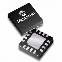
IC,Battery Management,LLCC,16PIN,PLASTIC
Manufacturer
Microchip Technology
Specifications of MCP73863-I/ML
Function
Charge Management
Battery Type
Lithium-Ion (Li-Ion), Lithium-Polymer (Li-Pol)
Voltage - Supply
4.5 V ~ 12 V
Operating Temperature
-40°C ~ 85°C
Mounting Type
Surface Mount
Package / Case
16-QFN
Output Voltage
4.1 V, 4.2 V
Output Current
1200 mA
Maximum Operating Temperature
+ 85 C
Minimum Operating Temperature
- 40 C
Mounting Style
SMD/SMT
Lead Free Status / RoHS Status
Lead free / RoHS Compliant
Lead Free Status / RoHS Status
Lead free / RoHS Compliant, Lead free / RoHS Compliant
Available stocks
Company
Part Number
Manufacturer
Quantity
Price
Company:

Part Number:
MCP73863-I/ML
Manufacturer:
ADI
Quantity:
22


MCP73861/2/3/4
5.1.6
The MCP7386X monitors the battery voltage at the
V
terminal of the battery pack.
5.1.7
The battery charge control output is the drain terminal
of an internal P-channel MOSFET. The MCP7386X
provides constant current and voltage regulation to the
battery pack by controlling this MOSFET in the linear
region. The battery charge control output should be
connected to the positive terminal of the battery pack.
5.2
5.2.1
Two status outputs provide information on the state of
charge. The current-limited, open-drain outputs can be
used to illuminate external LEDs. Optionally, a pull-up
resistor can be used on the output for communication
with a host microcontroller.
state of the status outputs during a charge cycle.
TABLE 5-1:
DS21893D-page 18
Qualification
Preconditioning
Constant-
Current Fast
Charge
Constant-
Voltage
Charge
Complete
Fault
THERM Invalid
Disabled –
Sleep mode
Input Voltage
Disconnected
BAT3
CYCLE STAT1
Note:
CHARGE
pin. This input is tied directly to the positive
Digital Circuitry
BATTERY VOLTAGE SENSE (V
BATTERY CHARGE CONTROL
OUTPUT (V
CHARGE STATUS OUTPUTS
(STAT1, STAT2)
Off state: Open-drain is high-impedance
On state: Open-drain can sink current
Flashing: Toggles between off state and
STATUS OUTPUTS (NOTE)
50% duty cycle)
Flashing (1 Hz,
(MCP73861/2)
(MCP73863/4)
typically 7 mA
on state
STAT1
BAT1
Off
On
On
On
Off
Off
Off
Off
Off
Table 5-1
, V
BAT2
50% duty cycle)
Flashing (1 Hz,
)
summarizes the
(All Devices)
STAT2
Off
Off
Off
Off
Off
On
Off
Off
BAT3
)
The flashing rate (1 Hz) is based off a timer capacitor
(C
value of the timer capacitor.
During a fault condition, the STAT1 status output will be
off and the STAT2 status output will be on. To recover
from a fault condition, the input voltage must be
removed and then reapplied, or the enable input (EN)
must be de-asserted to a logic-low, then asserted to a
logic-high.
When the voltage on the THERM input is outside the
preset window, the charge cycle will not start, or will be
suspended. The charge cycle is not terminated and
recovery is automatic. The charge cycle will resume (or
start) once the THERM input is valid and all other
qualification parameters are met. During an invalid
THERM condition, the STAT1 status output will be off
and the STAT2 status output will flash.
5.2.2
The V
the MCP7386X. With V
3 and MCP73862/4 regulate to 4.1V and 8.2V,
respectively. With V
and MCP73862/4 regulate to 4.2V and 8.4V,
respectively.
5.2.3
The logic enable input pin (EN) can be used to
terminate a charge at any time during the charge cycle,
as well as to initiate a charge cycle or initiate a recharge
cycle.
Applying a logic-high input signal to the EN pin, or tying
it to the input source, enables the device. Applying a
logic-low input signal disables the device and
terminates a charge cycle. When disabled, the device’s
supply current is reduced to 0.17 µA, typically.
TIMER
SET
) of 0.1 µF. The rate will vary based on the
input selects the regulated output voltage of
V
LOGIC ENABLE (EN)
SET
INPUT
SET
SET
© 2008 Microchip Technology Inc.
tied to V
tied to V
DD
SS
, the MCP73861/3
, the MCP73861/
Related parts for MCP73863-I/ML
Image
Part Number
Description
Manufacturer
Datasheet
Request
R

Part Number:
Description:
IC CONTROLLER LI-ION 4.5V 16SOIC
Manufacturer:
Microchip Technology
Datasheet:

Part Number:
Description:
Advanced Single or Dual Cell, Fully Integrated Li-Ion / Li-Polymer Charge Management Controllers
Manufacturer:
Microchip Technology

Part Number:
Description:
Manufacturer:
Microchip Technology Inc.
Datasheet:
Part Number:
Description:
Manufacturer:
Microchip Technology Inc.
Datasheet:
Part Number:
Description:
Manufacturer:
Microchip Technology Inc.
Datasheet:
Part Number:
Description:
Manufacturer:
Microchip Technology Inc.
Datasheet:
Part Number:
Description:
Manufacturer:
Microchip Technology Inc.
Datasheet:
Part Number:
Description:
Manufacturer:
Microchip Technology Inc.
Datasheet:
Part Number:
Description:
Manufacturer:
Microchip Technology Inc.
Datasheet:
Part Number:
Description:
Manufacturer:
Microchip Technology Inc.
Datasheet: