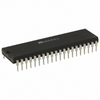
MM5450BN Micrel Inc, MM5450BN Datasheet - Page 4

MM5450BN
Manufacturer Part Number
MM5450BN
Description
LED Driver IC
Manufacturer
Micrel Inc
Datasheet
1.MM5451YV_TR.pdf
(9 pages)
Specifications of MM5450BN
Output Current
2.7mA
Operating Temperature Range
-40°C To +85°C
Driver Case Style
DIP
Device Type
LED
No. Of Pins
40
Mounting Type
Through Hole
Supply Voltage Min
4.75V
Output Current Max
25mA
No. Of Segments
7
Display Type
LED
Interface
Serial
Current - Supply
10mA
Voltage - Supply
4.75 V ~ 11 V
Operating Temperature
-40°C ~ 85°C
Package / Case
40-DIP (0.600", 15.24mm)
Lead Free Status / RoHS Status
Contains lead / RoHS non-compliant
Configuration
-
Digits Or Characters
-
Lead Free Status / RoHS Status
Contains lead / RoHS non-compliant, Contains lead / RoHS non-compliant
Available stocks
Company
Part Number
Manufacturer
Quantity
Price
Company:
Part Number:
MM5450BN
Manufacturer:
NSC
Quantity:
1 235
Company:
Part Number:
MM5450BN
Manufacturer:
NS
Quantity:
11 260
Part Number:
MM5450BN
Manufacturer:
MICROCH
Quantity:
20 000
Absolute Maximum Ratings
Voltage (any pin) ........................................V
Power Dissipation
Junction Temperature (T
Storage Temperature (T
Lead Temperature (soldering, 10sec.) ..................... +300°C
Electrical Characteristics
4.5V ≤ V
Notes:
1. Output matching is calculated as the percent variation (I
2. With a fixed resistor on the brightness input pin, some variation in brightness will occur among devices.
3. See Figures 7, 8 and 9 for recommended operating conditions and limits. Absolute maximum for each output should be limited to 40mA.
4. V
5. AC input waveform specification for test purpose: t
6. Clock input rise and fall times must not exceed 300ns.
Micrel, Inc.
Symbol
V
V
f
t
t
t
t
t
February 2006
C
H
L
DS
DH
DES
L
H
OUT
+25°C........................................................................1W
+85°C.................................................................560mW
should be regulated by user. See Figures 8 and 9 for allowable V
DD
≤ 11V, V
Parameter
Power Supply Current
Data Input Voltage
Brightness Control Input Current
Output Sink Current
Brightness Control Input Voltage
Output Matching
Clock Input Frequency
Clock Input High Time
Clock Input Low Time
Data Input Setup Time
Data Input Hold Setup Time
Data Enable Input Setup Time
Reset Pad Current
SS
= 0V; T
S
J
).........................–65°C to +150°C
) ....................................... +150°C
A
= 25°C, bold values indicate –40°C ≤ T
R
SS
≤ 200ns, t
to V
MAX
Condition
–25°C to +85°C, excluding output loads
–40°C to +85°C, excluding output loads
logic-0 level, ±10 µA input bias
logic-1 level, 4.75V ≤ V
V
Note 2
segment off, V
segment on, V
brightness input = 0µA
brightness input = 100µA
brightness input = 750µA
input current = 750 µA
Note 1
Notes 5, 6
Notes 5, 6
Notes 5, 6
die
DD
+ I
SS
> 5.25V
MIN
F
+ 12V
≤ 20ns, f = 500kHz, 50% ±10% duty cycle.
) / 2.
OUT
OUT
OUT
vs. I
4
Operating Ratings
Supply voltage (V
Ambient Temperature Range (T
= 3.0V
= 1.8V, Note 3
OUT
operation.
DD
A
≤ 5.25V
≤ +85°C, unless otherwise noted.
DD
– V
SS
).......................... +4.75V to +11V
V
–0.3
Min
DD
950
950
300
300
100
2.2
2.0
3.0
15
0
0
8
–2
A
) ............. –40°C to +85°C
Typ
2.7
MM5450/5451
(408) 955-1690
M9999-021606
Max
0.75
V
V
±20
500
8.5
0.8
4.3
10
10
10
25
4
8
DD
DD
Units
kHz
mA
mA
mA
mA
mA
µA
µA
µA
ns
ns
ns
ns
ns
%
V
V
V
V


