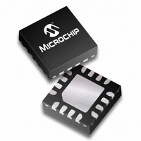
PIC16F610-E/ML Microchip Technology, PIC16F610-E/ML Datasheet - Page 166

PIC16F610-E/ML
Manufacturer Part Number
PIC16F610-E/ML
Description
1.75KB Flash, 64B RAM, 6 I/O, 8MHz Internal Oscillator 16 QFN 4x4mm TUBE
Manufacturer
Microchip Technology
Series
PIC® 16Fr
Datasheets
1.PIC12F609T-ISN.pdf
(26 pages)
2.PIC16F616T-ISL.pdf
(214 pages)
3.PIC16F616T-ISL.pdf
(8 pages)
Specifications of PIC16F610-E/ML
Core Processor
PIC
Core Size
8-Bit
Speed
20MHz
Peripherals
Brown-out Detect/Reset, POR, PWM, WDT
Number Of I /o
11
Program Memory Size
1.75KB (1K x 14)
Program Memory Type
FLASH
Ram Size
64 x 8
Voltage - Supply (vcc/vdd)
2 V ~ 5.5 V
Oscillator Type
Internal
Operating Temperature
-40°C ~ 125°C
Package / Case
16-QFN
Lead Free Status / RoHS Status
Lead free / RoHS Compliant
For Use With
AC162083 - HEADER MPLAB ICD2 PIC16F616 8/14AC164324 - MODULE SKT FOR MPLAB 8DFN/16QFNXLT16QFN1 - SOCKET TRANSITION 14DIP TO 16QFN
Eeprom Size
-
Data Converters
-
Connectivity
-
Lead Free Status / RoHS Status
Lead free / RoHS Compliant, Lead free / RoHS Compliant
- Current page: 166 of 214
- Download datasheet (4Mb)
PIC16F610/616/16HV610/616
TABLE 15-12: PIC16F616/16HV616 A/D CONVERSION REQUIREMENTS
DS41288F-page 166
Standard Operating Conditions (unless otherwise stated)
Operating temperature
AD130* T
AD131 T
AD132* T
AD133* T
AD134 T
Note 1:
Param
No.
2:
*
† Data in “Typ” column is at 5.0V, 25°C unless otherwise stated. These parameters are for design guidance
Sym
AD
CNV
ACQ
AMP
GO
These parameters are characterized but not tested.
only and are not tested.
ADRESH and ADRESL registers may be read on the following T
See Section 9.3 “A/D Acquisition Requirements” for minimum conditions.
A/D Clock Period
A/D Internal RC
Oscillator Period
Conversion Time
(not including
Acquisition Time)
Acquisition Time
Amplifier Settling Time
Q4 to A/D Clock Start
Characteristic
-40°C ≤ T
(1)
A
≤ +125°C
Min
1.6
3.0
3.0
1.6
—
—
—
—
T
OSC
T
Typ†
OSC
11.5
6.0
4.0
/2 + T
—
—
11
—
/2
CY
Max Units
9.0
9.0
9.0
6.0
—
—
—
—
5
T
μs
μs
μs
μs
μs
μs
—
—
AD
CY
T
T
ADCS<1:0> = 11 (ADRC mode)
At V
At V
Set GO/DONE bit to new data in A/D
Result register
If the A/D clock source is selected as
RC, a time of T
A/D clock starts. This allows the SLEEP
instruction to be executed.
OSC
OSC
cycle.
DD
DD
-based, V
-based, V
= 2.5V
= 5.0V
© 2009 Microchip Technology Inc.
Conditions
REF
REF
CY
≥ 3.0V
is added before the
full range
Related parts for PIC16F610-E/ML
Image
Part Number
Description
Manufacturer
Datasheet
Request
R

Part Number:
Description:
IC PIC MCU FLASH 1KX14 14DIP
Manufacturer:
Microchip Technology
Datasheet:

Part Number:
Description:
IC PIC MCU FLASH 1KX14 16QFN
Manufacturer:
Microchip Technology
Datasheet:

Part Number:
Description:
IC PIC MCU FLASH 1KX14 14SOIC
Manufacturer:
Microchip Technology
Datasheet:

Part Number:
Description:
IC PIC MCU FLASH 1KX14 14TSSOP
Manufacturer:
Microchip Technology
Datasheet:

Part Number:
Description:
1.75KB Flash, 64B RAM, 6 I/O, 8MHz Internal Oscillator 14 PDIP .300in TUBE
Manufacturer:
Microchip Technology
Datasheet:

Part Number:
Description:
1.75KB Flash, 64B RAM, 6 I/O, 8MHz Internal Oscillator 14 SOIC .150in TUBE
Manufacturer:
Microchip Technology
Datasheet:

Part Number:
Description:
1.75KB Flash, 64B RAM, 6 I/O, 8MHz Internal Oscillator 14 TSSOP 4.4mm TUBE
Manufacturer:
Microchip Technology
Datasheet:

Part Number:
Description:
IC, 8BIT MCU, PIC16F, 32MHZ, SOIC-18
Manufacturer:
Microchip Technology
Datasheet:

Part Number:
Description:
IC, 8BIT MCU, PIC16F, 32MHZ, SSOP-20
Manufacturer:
Microchip Technology
Datasheet:

Part Number:
Description:
IC, 8BIT MCU, PIC16F, 32MHZ, DIP-18
Manufacturer:
Microchip Technology
Datasheet:

Part Number:
Description:
IC, 8BIT MCU, PIC16F, 32MHZ, QFN-28
Manufacturer:
Microchip Technology
Datasheet:

Part Number:
Description:
IC, 8BIT MCU, PIC16F, 32MHZ, QFN-28
Manufacturer:
Microchip Technology
Datasheet:

Part Number:
Description:
IC, 8BIT MCU, PIC16F, 32MHZ, QFN-28
Manufacturer:
Microchip Technology
Datasheet:

Part Number:
Description:
IC, 8BIT MCU, PIC16F, 32MHZ, SSOP-20
Manufacturer:
Microchip Technology
Datasheet:

Part Number:
Description:
IC, 8BIT MCU, PIC16F, 20MHZ, DIP-40
Manufacturer:
Microchip Technology
Datasheet:


